Method of forming an N channel and P channel finfet device on the same semiconductor substrate

a technology of finfet and semiconductor substrate, which is applied in the direction of semiconductor devices, electrical equipment, transistors, etc., can solve the problems of difficult to achieve the finfet type device, device, comprised of both nmos and pmos devices, and achieve gate resistance reduction

Inactive Publication Date: 2007-03-06
TAIWAN SEMICON MFG CO LTD
View PDF6 Cites 52 Cited by
  • Summary
  • Abstract
  • Description
  • Claims
  • Application Information

AI Technical Summary

Benefits of technology

[0012]A second embodiment of this invention entails the use of dummy fin structures located between the NMOS and PMOS fin structures, allowing the deposition of the material used for the conduc

Problems solved by technology

The ability to fabricate a complimentary metal oxide semiconductor (CMOS), device, compris

Method used


Image

  • Method of forming an N channel and P channel finfet device on the same semiconductor substrate
  • Method of forming an N channel and P channel finfet device on the same semiconductor substrate
  • Method of forming an N channel and P channel finfet device on the same semiconductor substrate

Examples


Embodiment Construction

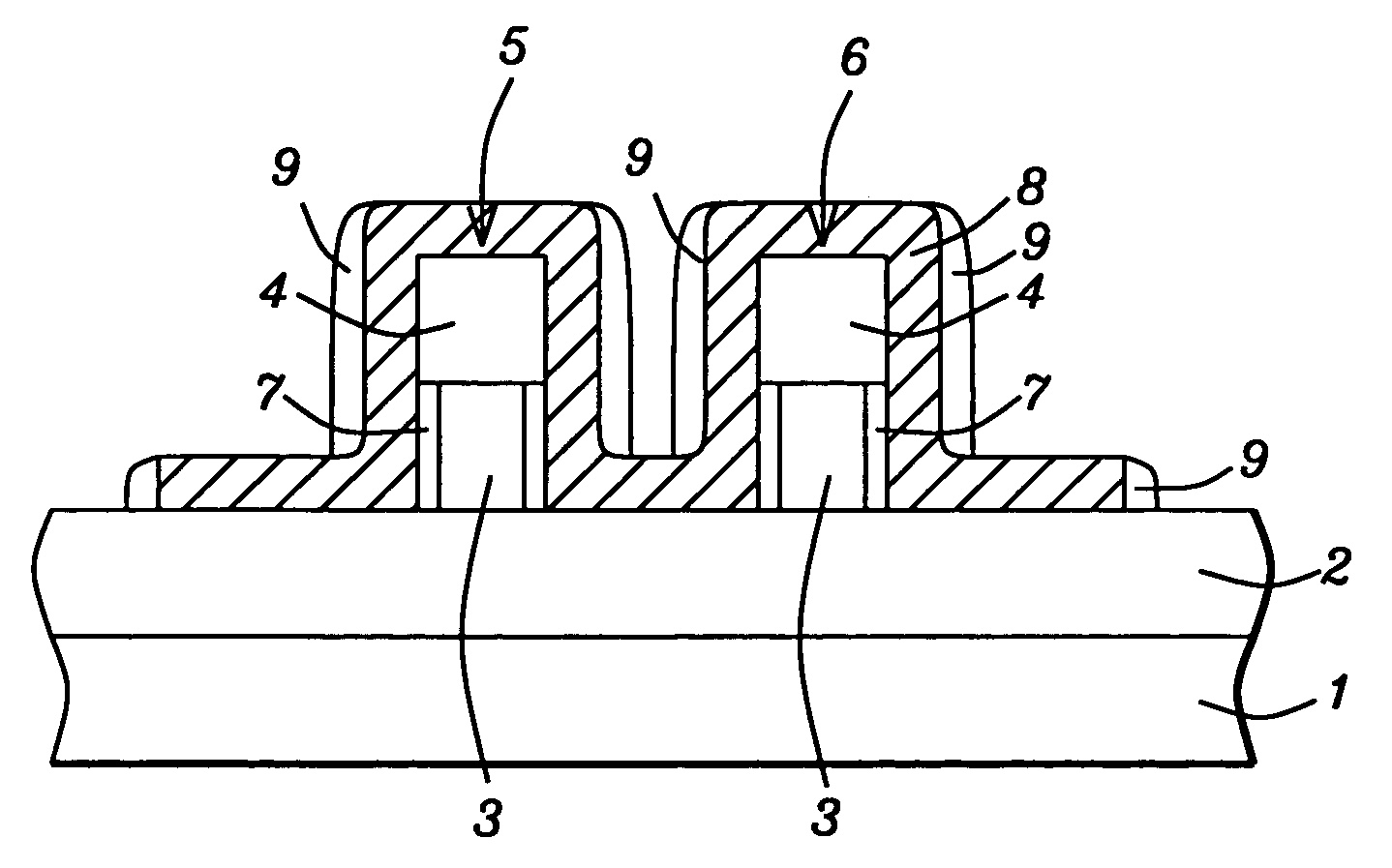
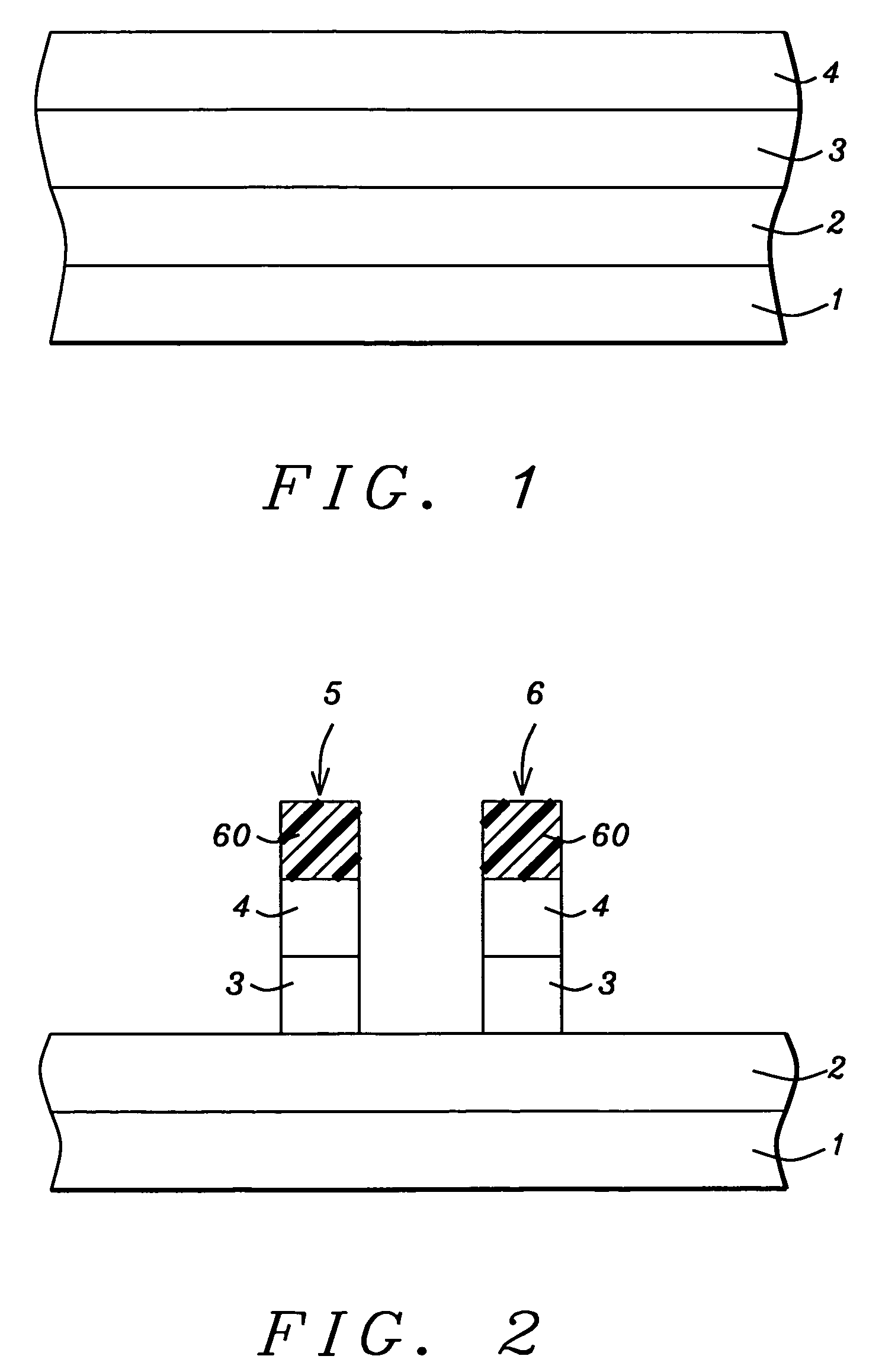
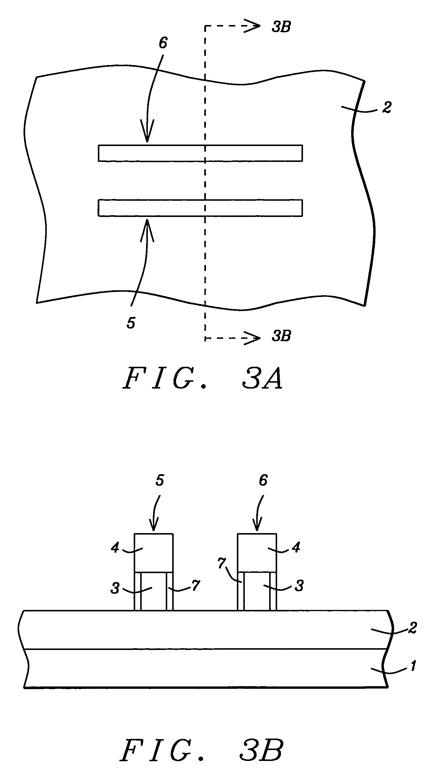
[0016]The method of forming an NMOS FINFET device, and a PMOS FINFET device, in the same SOI layer, featuring reductions in source / drain and gate resistance, will now be described in detail. Semiconductor substrate 1, comprised of single crystalline silicon with a crystallographic orientation, is used and schematically shown in FIG. 1. Silicon layer 3, the silicon component of an SOI layer, is formed via oxygen implantation into a portion of semiconductor substrate 1, followed by an anneal procedure which results in the formation of insulator layer 2, underlying non-implanted, and non-oxidized silicon layer 3. Insulator layer 2, is comprised of silicon dioxide at a thickness between about 100 to 1000 Angstroms, while SOI layer 3, the remaining top portion of semiconductor substrate 1, overlying insulator layer 2, is maintained at a thickness between about 50 to 5000 Angstroms. If desired the SOI configuration can be obtained via bonding of a first semiconductor substrate to the top...


PUM


Abstract

A method of forming a FINFET CMOS device structure featuring an N channel device and a P channel device formed in the same SOI layer, has been developed. The method features formation of two parallel SOI fin type structures, followed by gate insulator growth on the sides of the SOI fin type structures, and definition of a conductive gate structure formed traversing the SOI fin type structures while interfacing the gate insulator layer. A doped insulator layer of a first conductivity type is formed on the exposed top surfaces of a first SOI fin type shape, while a second doped insulator layer of a second conductivity type is formed on the exposed top surfaces of the second SOI fin type shape. An anneal procedure results creation of a source/drain region of a first conductivity type in portions of the first SOI fin type shape underlying the first doped insulator layer, and creation of a source/drain region of a second conductivity type in portions of the second SOI fin type shape underlying the second doped insulator layer. Selective deposition of tungsten on exposed top surface of the source/drain regions is then employed to decrease source/drain resistance.

Description

[0001]This is a division of patent aqpplication Ser. No. 10 / 235,253, filing date Sep. 5, 2002 now U.S. Pat. No. 6,770,516, Method Of Forming An N Channel And P Channel Finfet Device On The Same Semiconductor Substrate, assigned to the same assignee as the present invention, which is herein incorporated by reference in its entirety.BACKGROUND OF THE INVENTION[0002](1) Field of the Invention[0003]The present invention relates to methods used to fabricate semiconductor devices, and more specifically to a method used to fabricate a fin type field effect transistor (FINFET) device on a semiconductor substrate.[0004](2) Description of Prior Art[0005]Micro-miniaturization, the ability to fabricate semiconductor devices comprised with sub-micron features, has allowed the performance of devices comprised with the sub-micron features to be increased. In addition the use of sub-micron features has allowed the attainment of smaller semiconductor chips to be realized, still providing device dens...

Claims


Application Information

Patent Timeline
IPC IPC(8): H01L29/76H01L21/336H01L21/84H01L27/12H01L29/423H01L29/786
CPCH01L21/84H01L27/1203H01L29/66795H01L29/785H01L29/42384Y10S438/962H01L29/6681
Inventor WU, CHUNG-CHENGWU, SHYE-LIN
Owner TAIWAN SEMICON MFG CO LTD
Why Eureka
Try Eureka