Read out scheme for several bits in a single MRAM soft layer

a soft layer and readout technology, applied in the field of magnetic memory cells, can solve the problems of high energy consumption, loss of stored data, and moderate cost of drams, and achieve the effect of reducing manufacturing cost and increasing memory density

Inactive Publication Date: 2007-03-06
INFINEON TECH AG
View PDF9 Cites 17 Cited by
  • Summary
  • Abstract
  • Description
  • Claims
  • Application Information

AI Technical Summary

Benefits of technology

[0019]In one aspect, the present invention relates to utilizing the resistance characteristics of MTJ devices, including devices based on GMR or another mechanism in which a resistance is dependent on the direction of polarization of a free magnetic layer with respect to at least two fixed magnetic layers, that can exhibit at least four distinct resistance values dependent on the magnetic orientation of a magnetic layer so that at least two bits of data can be stored and read. In response to the diminishing activation energy of an MTJ cell as the cell volume is decreased with the utilization of extremely small feature sizes, the present invention provides an MRAM device capable of storing a plurality of bits of information in a single cell. Thereby the design and efficient manufacture of high density and low cost MTJ memory devices is enabled.
[0020]Embodiments of the present invention achieve technical advantages by configuring an MTJ device with two fixed layers with a magnetic orientation of one fixed layer at an angle with respect to the magnetic orientation of the other fixed layer, and with orientations of the fixed magnetic layers that are neither parallel nor antiparallel. Preferably, the angle between the magnetic orientations of the fixed layers is 90 degrees. In a further embodiment, the fixed layers are ferromagnetic layers formed as thin films on an insulating surface. In a further embodiment an antiferromagnetic layer is formed adjacent to each fixed layer. In a further embodiment a free ferromagnetic layer is formed between the fixed layers and is separated from each fixed magnetic layer by an insulating layer. Preferably, the free ferromagnetic layer is formed with a soft ferromagnetic material. Preferably, the free ferromagnetic layer exhibits four stable magnetic orientations. In an embodiment of the present invention the free layer is configured as a synthetic antiferromagnetic layer including multiple antiferromagnetically coupled layers of a ferromagnetic material with an antiferromagnetic coupling spacer layer between each antiferromagnetic layer. Preferably, the thickness of each insulating layer is chosen to provide distinguishable resistances for the MTJ stack depending on the orientation of the free magnetic layer so that the stable orientations of the free magnetic layer can be uniquely sensed from the MTJ stack resistance. The thickness of one insulating layer is preferably greater than the thickness of the other to provide distinguishable resistances. Alternatively, one insulating layer is formed with a material composition different from that of the other to provide distinguishable resistances. Preferably the MTJ is formed in a lobed pattern with even symmetry. In a further embodiment bit lines, word lines and read word lines are formed adjacent to an array of MTJ cells so that individual MTJ cells in an array can be programmed and read. Preferably, to program an MTJ stack, the bit lines and word lines are driven with controlled currents of sufficient magnitude and duration to selectively reorient the direction of the magnetic field of the free layer. Preferably, a sense amplifier capable of distinguishing at least four resistance states is configured to read the cell data. Preferably, the sense amplifier is a current sense amplifier.
[0026]Embodiments of the present invention achieve technical advantages as a memory device including MTJ cells each storing a plurality of bits of information. Advantages of embodiments of the present invention include a memory device with increased memory density and reduced manufacturing cost, that is non-volatile upon removal of electrical power, and that does not require its data to be re-written after it has been read.

Problems solved by technology

DRAMs have moderate cost, are very fast and can have access times on the order of about 30 nanoseconds, but lose the stored data upon loss of electrical power, i.e., they are “volatile”.
Further application considerations for each technology include limitations on the number of times a memory cell can be written or read before it deteriorates, how long it reliably retains data, its data storage density, how much energy it consumes, the need for integral mechanical devices such as for disk drives and tapes, and the complexity and expense of associated circuitry.
Considering these limitations, there is now no ideal technology for general applications.
Opto-isolators are often limited in performance by a maximum data rate due in part to their ability to transmit one bit of data at a time.
When substantial data must be communicated quickly, multiple opto-isolators are often required, which can consume valuable circuit-board space.
However, a limitation of a magnetic tunnel junction cell as described above is its ability to be programmed with only a single bit of information, a limitation shared with memory elements that are based on charge storage such as a DRAM or on switching transistor pairs such as in a static RAM (SRAM).
This one-bit limitation of magnetic tunnel junction cells arises from the two stable magnetic orientations of its free magnetic layer, whereby one orientation is utilized to represent a “0”, and the other, a “1”.
However, the activation energy of a cell varies as the cell volume, and consequently, with a small energy barrier inherently associated with small cells, random loss of data can occur in cells that are too small due to the stochastic processes associated with ordinary thermal effects.

Method used


Image

  • Read out scheme for several bits in a single MRAM soft layer
  • Read out scheme for several bits in a single MRAM soft layer
  • Read out scheme for several bits in a single MRAM soft layer

Examples


Embodiment Construction

[0039]The making and using of the presently preferred embodiments are discussed in detail below. It should be appreciated, however, that the present invention provides many applicable inventive concepts that can be embodied in a wide variety of specific contexts. The specific embodiments discussed are merely illustrative of specific ways to make and use the invention, and do not limit the scope of the invention.

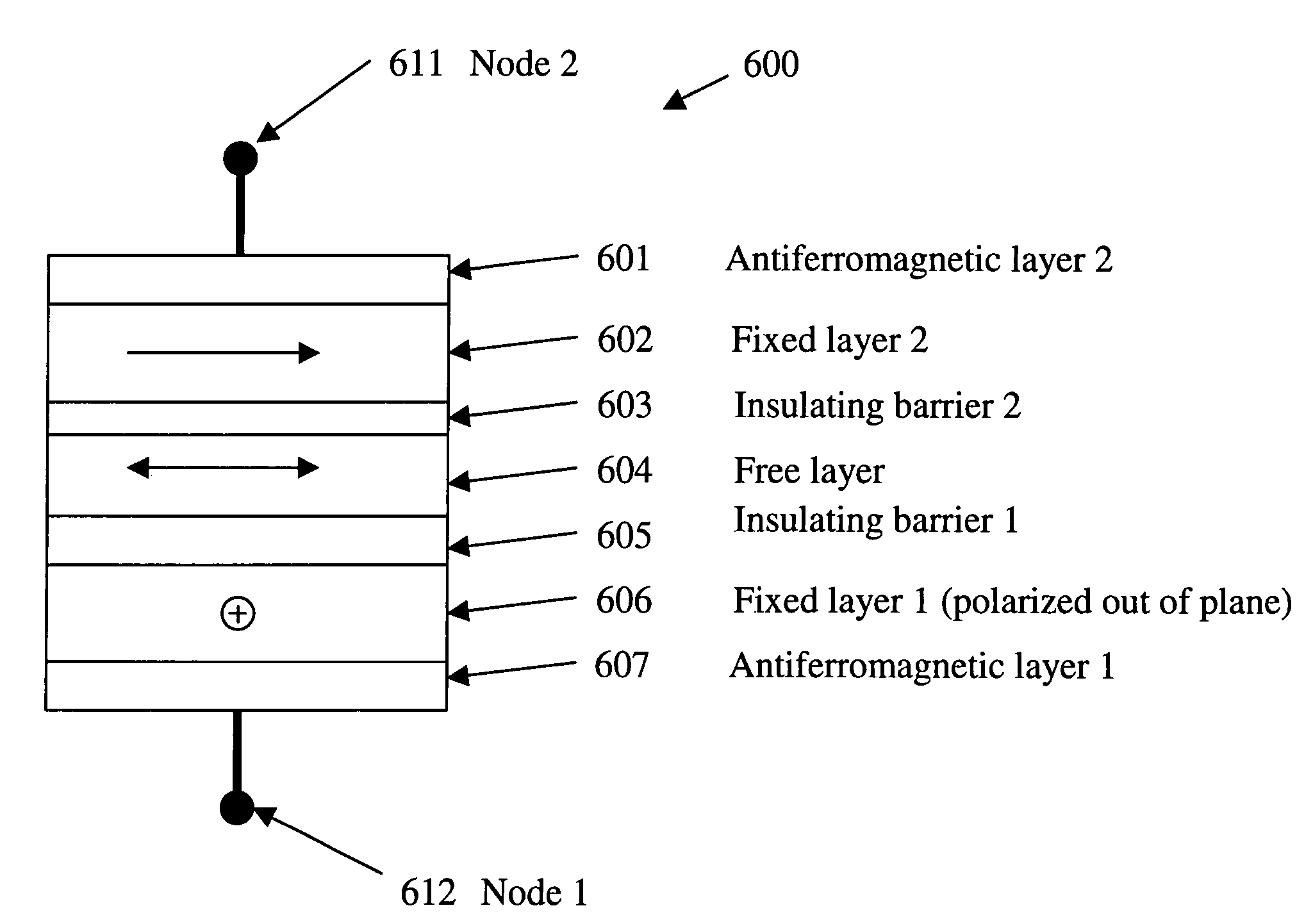
[0040]Embodiments of the present invention will be described with respect to preferred embodiments in a specific context, namely a FET MRAM device configured to store (or be programmed with) a plurality of bits. The invention may be applied to resistive memory devices and other memory devices that include a plurality of current sense amplifiers and reference current sources to detect the resistive state of memory cells configured to store a plurality of bits.

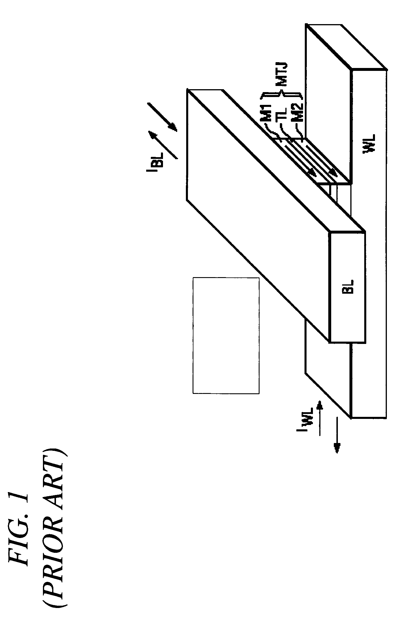
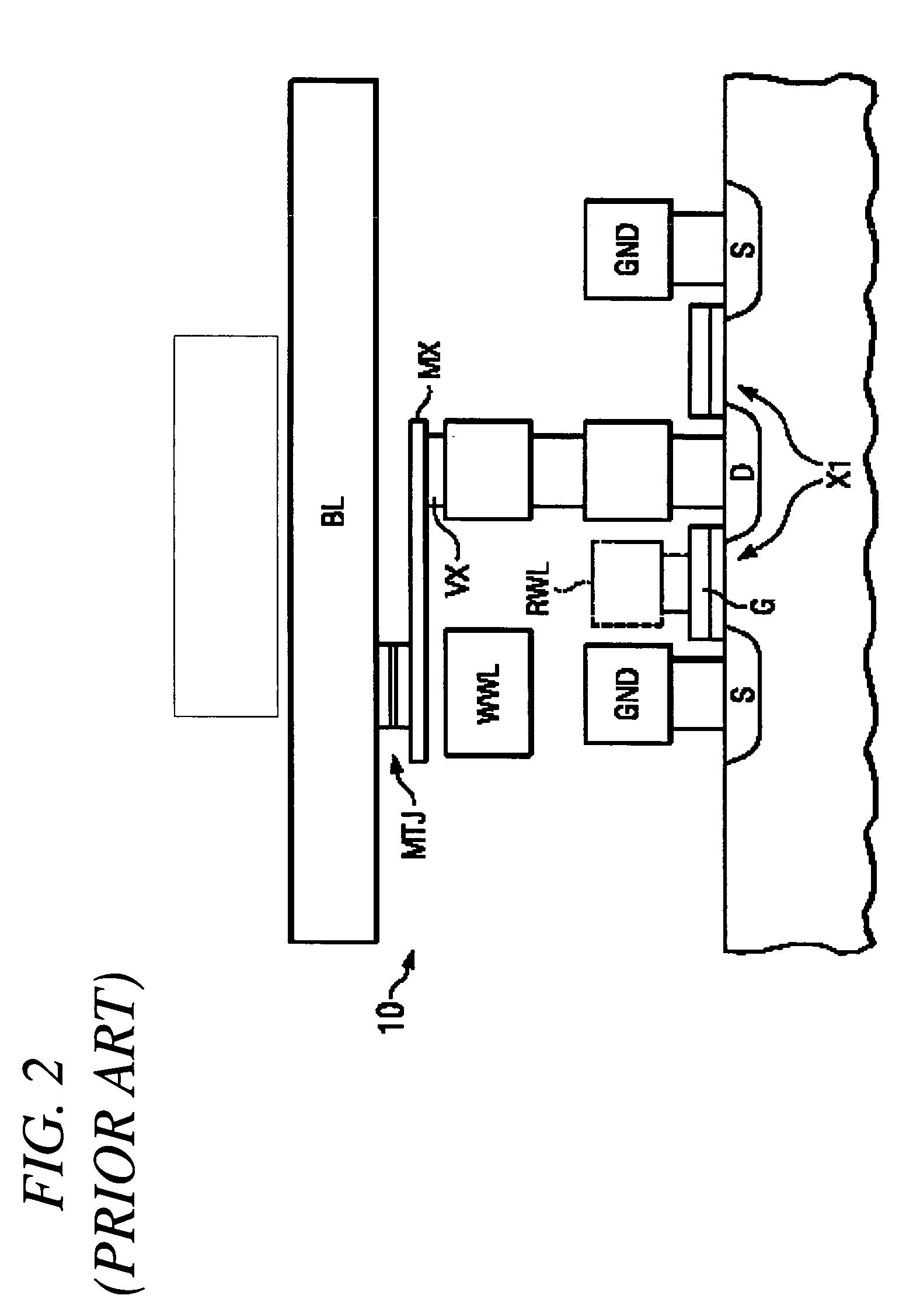
[0041]In resistive memory devices such as MRAMs, even in MRAMs storing only one bit, a current sensing circuit includin...


PUM


Abstract

A magnetic tunnel junction (MTJ) device is configured to store at least two bits of data in a single cell utilizing the variable resistance characteristic of a MTJ. The MTJ includes a soft and two fixed magnetic layers with fixed field directions oriented in perpendicular directions. The soft magnetic layer is separated from the fixed layers by insulating layers preferably with different thicknesses, or with different material compositions. The resulting junction resistance can exhibit at least four distinct resistance values dependent on the magnetic orientation of the free magnetic layer. The cell is configured using a pattern with four lobes to store two bits, and eight lobes to store three bits. The resulting cell can be used to provide a fast, non-volatile magnetic random access memory (MRAM) with high density and no need to rewrite stored data after they are read, or as a fast galvanic isolator.

Description

[0001]This application claims the benefit of U.S. Provisional Application No. 60 / 589,116, filed on Jul. 19, 2004, entitled Read Out Scheme For Several Bits In A Single MRAM Soft Layer, which application is hereby incorporated herein by reference.CROSS-REFERENCE TO RELATED APPLICATIONS[0002]This application relates to co-pending and commonly assigned parent applications Ser. No. 10 / 326,367, filed Dec. 20, 2002, entitled “Current Sense Amplifier,” Ser. No. 10 / 937,155, filed Sep. 7, 2004, entitled “Current Sense Amplifier,” and Ser. No. 10 / 982,026, filed Nov. 4, 2004, entitled “Reference Current Source for Current Sense Amplifier and Programmable Resistor Configured with Magnetic Tunnel Junction Cells,” which applications are hereby incorporated herein by reference.TECHNICAL FIELD[0003]Embodiments of the present invention relate generally to using at least two fixed magnetic layers to store a plurality of bits in a single magnetic tunnel junction cell. In particular, embodiments of the...

Claims


Application Information

Patent Timeline
Patent Type & Authority Patents(United States)
IPC IPC(8): G11C11/00
CPCG11C11/15G11C11/5607G11C2211/5634
Inventor BRAUN, DANIELMUELLER, GERHARD
Owner INFINEON TECH AG
Why Eureka
Try Eureka