Processing high-speed digital signals

a digital signal and high-speed technology, applied in the direction of synchronising signal speed/phase control, generating/distributing signals, baseband system details, etc., can solve the problems of inability to guarantee, the above-mentioned data sample processing is also problematic at very high clock frequencies, and the enabling of different latches is no longer performed correctly

Active Publication Date: 2007-03-06
SOCIONEXT INC
View PDF17 Cites 72 Cited by
  • Summary
  • Abstract
  • Description
  • Claims
  • Application Information

AI Technical Summary

Benefits of technology

[0025]Such verification circuitry can be implemented simply using only simple combinatorial logic gates such as AND or NAND gates and an exclusive OR gate. Furthermore, the loading imposed on the circulating control register by the circuitry can be desirably low, so that high-speed operation is not compromised.
[0032]Because the offset clock signal is selected from amongst the candidate clock signals it can be selected using a control signal provided from outside the circuitry. This makes the circuitry highly flexible.
[0034]Preferably, the selection signals used to designate one or both of the candidate clock signals selected as the recovered clock signal and the offset clock signal is / are Gray-coded signals so that unnecessary transitory phase jumps are avoided when the candidate clock signal selections are changed. For the same reason it is preferable that the first and last candidate clock signals of the plurality differ in phase from one another by substantially the same amount as the two candidate clock signals of each further pair of mutually-adjacent candidate clock signals of the plurality differ in phase from one another.

Problems solved by technology

When the frequency of the recovered clock signal (clock frequency) is high, bordering on the maximum speed of operation of the circuit elements making up the clock recovery circuitry, several design problems arise, as follows.
Firstly, the clock recovery circuitry will require signals which change at certain well-defined moments.
With such a previously-considered reset circuit, however, it is found that at frequencies approaching the limit of the technology, it is not possible to guarantee in which half of the clock cycle a reset signal produced by the reset circuit will switch from one logical state to the other.
This problem arises as the switching time of a master-slave latch varies due to manufacturing or processing tolerances, voltage margins and temperature variations (so-called PVT variation).
Secondly, the processing of the above-mentioned data samples is also problematic at very high clock frequencies.
At frequencies bordering on the limit of the technology, this can be very difficult.
In practice, however, the circulating control sequence may become corrupted, with the result that the enabling of the different latches is no longer performed correctly.
However, as the length of the control sequence increases (for example to 8 bits or more), the detection of the correct control states becomes more difficult.
In particular, more gates are required to implement the circuitry for checking the correctness of the control states which inevitably leads to increased loads on the control-register outputs.
Fourthly, high-speed digital signal processing circuitry may also have a requirement to convert items of data in one form into items of data in another form.
At very high frequencies approaching the limit of the technology, it is very difficult to control the relative phase of the serial clock signal with respect to that of the parallel clock signal (i.e. across all PVT and layout variations).
However, this has inherent disadvantages, and in particular the delay is hard to control across process, voltage and temperature variations.
Furthermore, such a delay element is difficult to control from outside the clock recovery circuitry and can only impose a delay (rather than an advance) relative to the recovered clock signal.

Method used


Image

  • Processing high-speed digital signals
  • Processing high-speed digital signals
  • Processing high-speed digital signals

Examples


Embodiment Construction

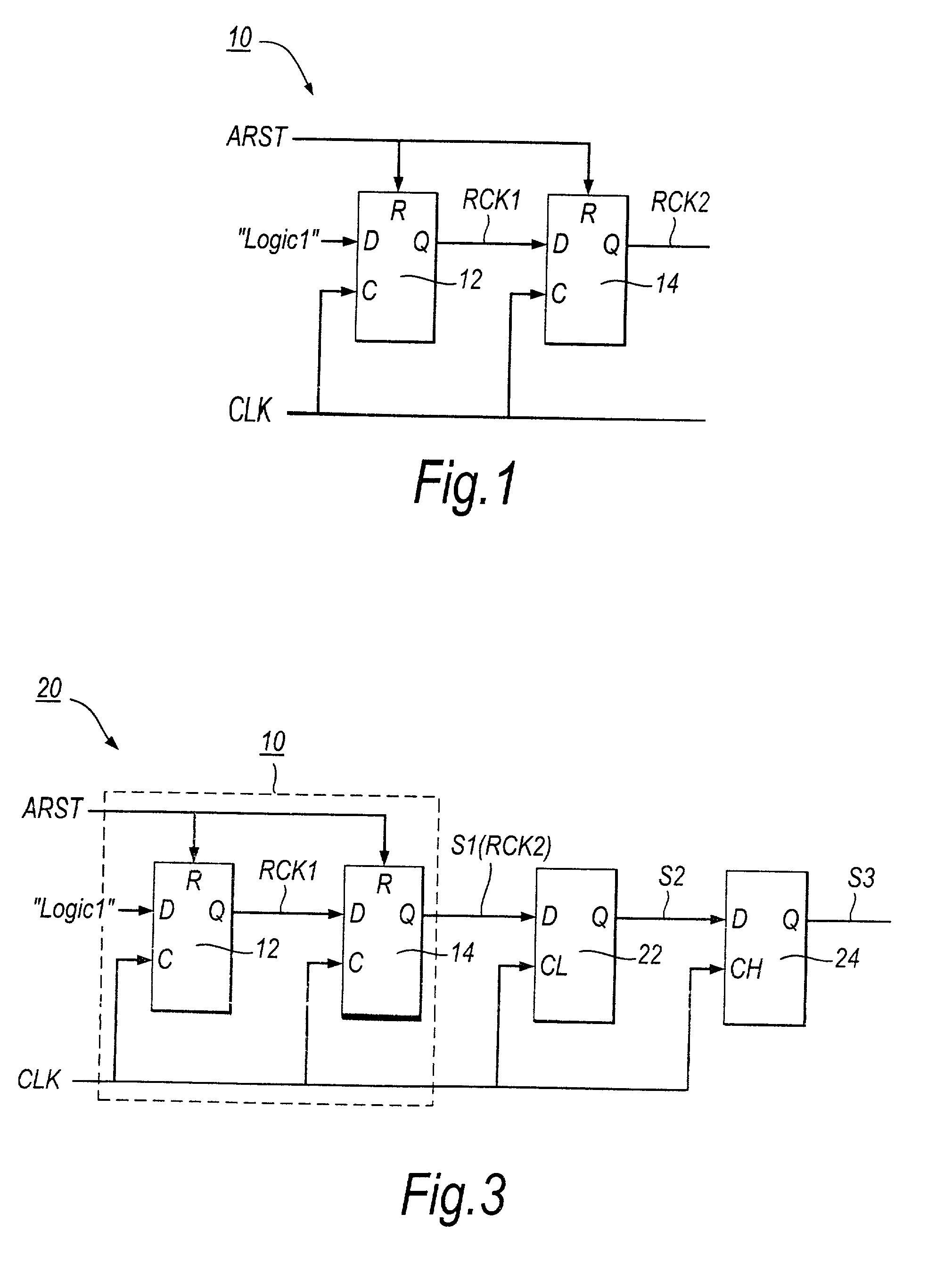
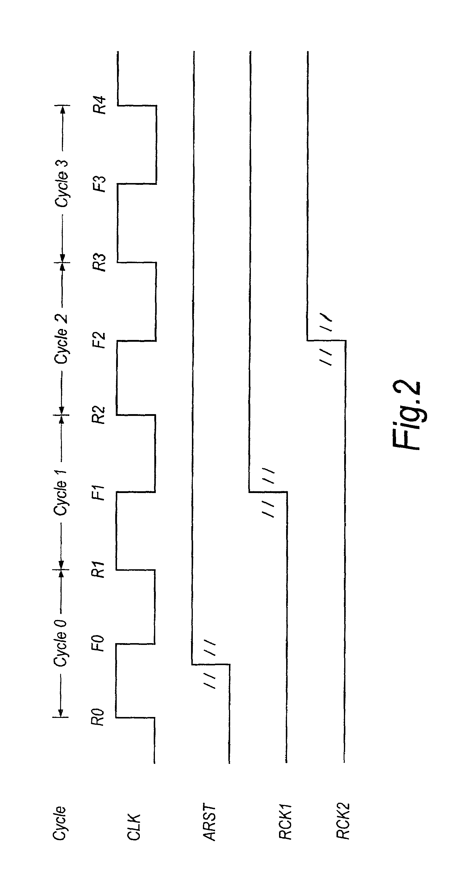
[0058]Before describing a preferred embodiment of the invention signal generating circuitry previously considered for use in clock recovery circuitry will be described with reference to FIGS. 1 and 2.

[0059]The previously-considered signal generating circuitry 10 shown in FIG. 1 comprises a first latch element 12 and a second latch element 14. Each of the latch elements 12 and 14 is, for example, a positive-edge-triggered master / slave D-type latch element.

[0060]Each of the latch elements 12 and 14 has a clock input C which is connected to receive a clock signal CLK. Each latch element 12 and 14 also has a reset input R which is connected to receive an active-low asynchronous reset signal ARST. The reset signal ARST is asynchronous with respect to the clock signal CLK. The first latch element 12 has a data input D which is connected to be at the high logic level H (logic 1). The second latch element 14 has a data input D connected to a data output Q of the first latch element 12 for r...


PUM


Abstract

A first transparent latch receives a first synchronised signal changing its logic state synchronously with respect to a clock signal. A second transparent latch receives a second synchronised signal output by the first latch. When the clock signal has a first logic state the first latch has a non-responsive state and the second latch has a responsive state, and when the clock signal has a second logic state the first latch has the responsive state and the second latch has the non-responsive state. The change in logic state of a third synchronised signal output by the second latch is guaranteed to occur in a particular half-cycle of the clock signal, irrespective of process / voltage / temperature (PVT) variations of the circuitry. Clock recovery circuitry may have rising-edge and falling-edge latches; circulating control pattern verification circuitry; data synchronising circuitry for converting parallel data clocked by a first clock signal into serial data clocked by a second clock signal asynchronous with the first clock signal; and data recovery circuitry for producing an offset clock signal which suits a data eye shape of a received serial data stream.

Description

BACKGROUND OF THE INVENTION[0001]1. Field of Invention[0002]The present invention relates to processing high-speed digital signals and, in particular but not exclusively, to processing high-speed digital signals to recover clock and / or data signals from received high-speed signals.[0003]2. Description of the Related Art[0004]Recovery of a clock signal from a serial data stream requires that data is latched (sampled) on both the rising and falling clock edges, the data samples then being processed to produce a recovered clock signal.[0005]When the frequency of the recovered clock signal (clock frequency) is high, bordering on the maximum speed of operation of the circuit elements making up the clock recovery circuitry, several design problems arise, as follows.[0006]Firstly, the clock recovery circuitry will require signals which change at certain well-defined moments. It may be necessary to control the moment a control signal such as a reset signal changes to an accuracy of half a c...

Claims


Application Information

Patent Timeline
Patent Type & Authority Patents(United States)
IPC IPC(8): H04L7/00G06F1/06H03L7/07H03L7/081H04L7/02H04L7/033H04L7/04H04L25/14
CPCH03L7/07H03L7/0814H04L25/14H04L7/041H04L7/033H03L7/0812
Inventor NAVEN, FINBARSOU, ANTONYRASHMAN, WAYNE ERIC
Owner SOCIONEXT INC
Why Eureka
Try Eureka