Amorphous silicon deposition for sequential lateral solidification

Inactive Publication Date: 2007-03-20
LG DISPLAY CO LTD
View PDF12 Cites 5 Cited by
  • Summary
  • Abstract
  • Description
  • Claims
  • Application Information

AI Technical Summary

Benefits of technology

[0027]An advantage of the present invention is to provide an amorphous silicon deposition method for sequential lateral solidification (SLS) that increases the process window.
[0028]Another advantage of the present invention is to provide an amorphous silicon deposition method for sequential lateral solidification (SLS) that increases the manufacturing yield and the product stability.

Problems solved by technology

However, amorphous silicon (a-Si) has problems when used in large-area LCD devices because the electrical characteristics of amorphous silicon are problematic.
However, polycrystalline silicon used in TFT switches and CMOS transistors have many crystal grains, and thus grain boundaries.
Those grains and boundaries interrupt carrier movement and cause deterioration of the active matrix elements.
Thus, a silicon crystallization method that produces large grains is an important issue.
However, since the plurality of seeds 13 are distributed randomly over the transparent substrate 1, it is difficult to obtain a plurality of uniform grains “G2” even though the grains “G2” are larger.
If the thickness of the amorphous silicon layer was greater than 500 angstroms, the laser beam would have to a greater laser density energy to melt the thicker amorphous silicon, which would increase manufacturing costs and possibly slow down the fabrication process, with no improvement in the characteristics of the thin film transistors being produced.
Since SLS crystallization uses a laser beam having an energy density sufficient to completely melt the silicon layer, the thickness of the amorphous silicon layer is an important issue.
If the amorphous silicon layer has a thickness of about 500 angstroms, defects occur during SLS crystallization.
Accordingly, 500 angstroms thick amorphous silicon has a narrow process window and is susceptible to defects.

Method used


Image

  • Amorphous silicon deposition for sequential lateral solidification
  • Amorphous silicon deposition for sequential lateral solidification
  • Amorphous silicon deposition for sequential lateral solidification

Examples


Embodiment Construction

[0042]Reference will now be made in detail to illustrated embodiments of the present invention, examples of which are shown in the accompanying drawings. Wherever possible, similar reference numbers will be used throughout the drawings to refer to the same or similar parts.

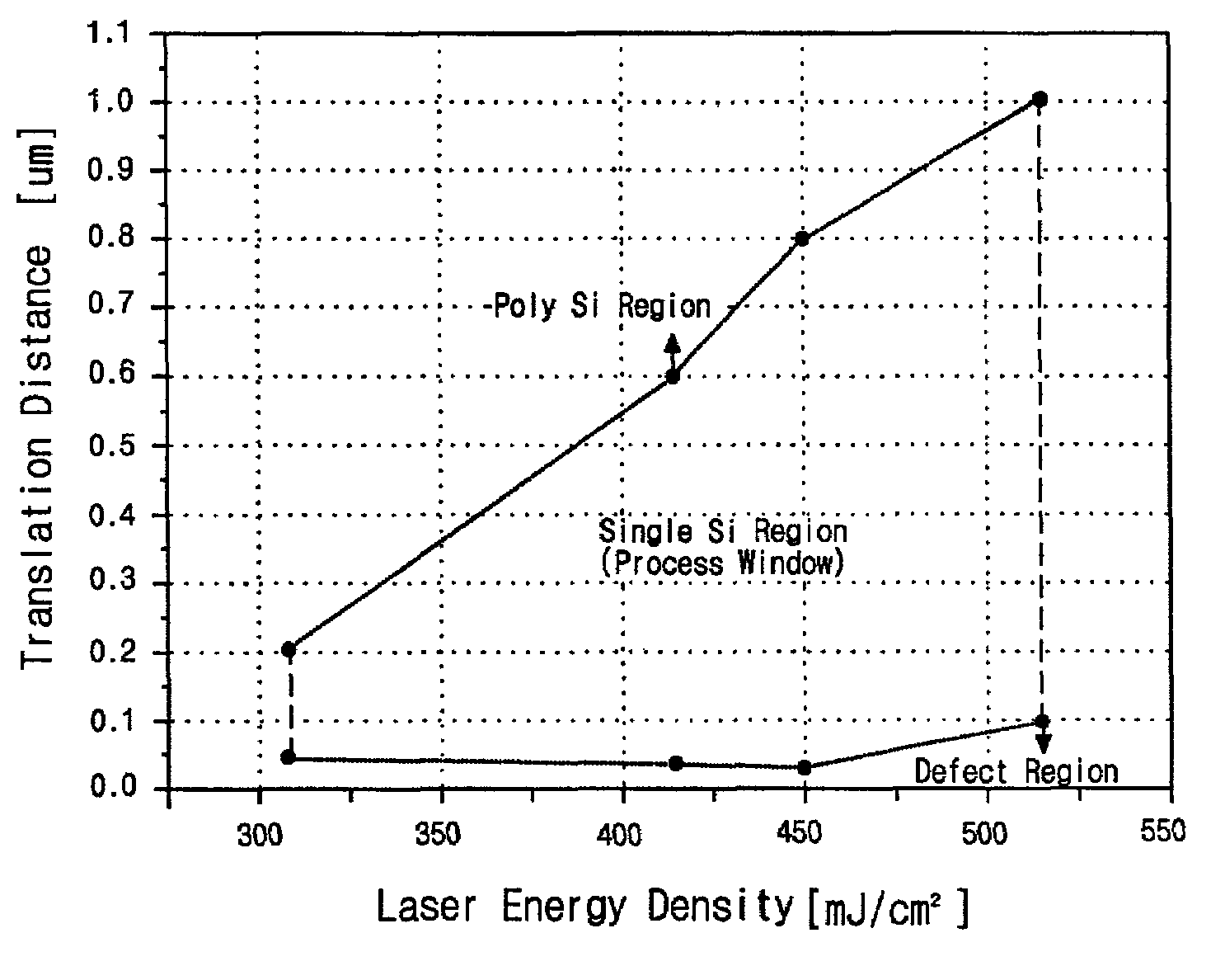
[0043]FIG. 6 is a graph showing a laser energy density that can frame a process window during SLS crystallization when the amorphous silicon layer has a thickness of 1,000 angstroms according to the present invention. When the laser energy density is 310 mJ / cm2, the maximum translation distance is 0.2 micrometers and the minimum translation distance is 0.05 micrometers. Laser energy density of 415 mJ / cm2 corresponds to a maximum translation distance of 0.6 and a minimum translation distance of 0.04 micrometers, the laser energy density of 450 mJ / cm2 corresponds to a maximum translation distance of 0.8 and a minimum of translation distance 0.04 micrometers, and a laser energy density of 515 mJ / cm2 corresponds to a ...


PUM


Abstract

An amorphous silicon deposition method includes the step of forming a buffer layer on a transparent substrate; depositing amorphous silicon on the buffer layer by a thickness ranging from 600 to 2,000 angstroms; repeatedly irradiating the amorphous silicon layer to completely melt using a laser beam that has a complete melting energy density; and moving the laser beam by a transaction distance for the next laser beam irradiation.

Description

[0001]This application claims the benefit of Korean Patent Application No. 2001-29885, filed on May 30, 2001 in Korea, which is hereby incorporated by reference as it sully set forth herein.BACKGROUND OF THE INVENTION[0002]1. Field of the Invention[0003]The present invention relates to an amorphous silicon deposition, and more particularly, to an amorphous silicon deposition method that is useful for sequential lateral solidification (SLS).[0004]2. Discussion of the Related Art[0005]Flat panel display devices that are thin, lightweight, and have low power consumption are in high demand. Flat panel display devices may be classified into two basic types. One type is a light-emitting display device that emits light to display images, and the other is a light-receiving display device that uses external light source to display images. Plasma display panels (PDPs), field emission display (FED) devices, and electro luminescence display devices are examples of light-emitting displays. Liqui...

Claims


Application Information

Patent Timeline
IPC IPC(8): B05D3/00C30B13/00G02F1/1368H01L21/20H01L21/205H01L21/268H01L21/336H01L29/786
CPCC30B13/00H01L21/2026C30B29/06H01L21/02598H01L21/02532H01L21/02675H01L21/02691H01L21/02595
Inventor JUNG, YUN-HO
Owner LG DISPLAY CO LTD
Why Eureka
Try Eureka