Method of manufacturing a multilayered doped conductor for a contact in an integrated circuit device

a technology of integrated circuit device and contact, which is applied in the direction of semiconductor/solid-state device details, instruments, marketing, etc., can solve the problems of increasing junction leakage, premature depletion of capacitor's stored charge, and mosfets becoming more susceptible to certain problems, and achieves high dopant concentration

Inactive Publication Date: 2007-03-27
MICRON TECH INC
View PDF13 Cites 36 Cited by
  • Summary
  • Abstract
  • Description
  • Claims
  • Application Information

AI Technical Summary

Benefits of technology

[0013]A memory device addressing reliability and refresh characteristics beyond that obtainable from prior art devices, as well as a method of fabricating such a device is described. In particular, the present invention addresses reliability in memory IC devices at burn-in, such for example DRAMs, having gate lengths less than 0.18 μm and a gate overlap less than 0.018 μm through the use of a multilayered doped conductor. The multilayered doped conductor creates a high dopant concentration in the active area close to the channel region. Because device degradation is due, at least in part, to increased trap states close to the channel region, the rich dopant layer created by the multilayered doped conductor is less susceptible to depletion of trapped charges in the oxide. This addresses device reliability at burn-in and lowers junction leakage, thereby permitting a longer period between refresh cycles.

Problems solved by technology

As the channel lengths of MOSFET devices have been reduced below 0.18 μm, MOSFETS have become more susceptible to certain problems.
One common problem is increased junction leakage I3, which affects the refresh characteristics of a dynamic random access memory (DRAM) cell.
Increased junction leakage leads to a premature depletion of the capacitor's stored charge, necessitating more frequent refresh cycles in such DRAM devices.
However, reducing the width of the gate overlap region is not without consequences.
In particular, reducing the width of the gate overlap region worsens the reliability of the DRAM device after a high voltage stress, such as experienced during burn-in.
This stress can lead to the premature failure of weaker devices, as the heat of burn-in causes ions in the active regions of each MOS transistor to dissipate to the point where the device can no longer function.
Further aggravating the problems associated with such devices with reduced overlap gate regions, is BPSG poisoning and access device n-sheet resistance.
However, TEOS liners can potentially increase the trapped states and interfacial charge density close to the source / drain regions.
Such diffusion also decreases device reliability due to hot carriers in compensated regions now having additional states to occupy, thereby further depleting the electron density in the active area of the device.

Method used


Image

  • Method of manufacturing a multilayered doped conductor for a contact in an integrated circuit device
  • Method of manufacturing a multilayered doped conductor for a contact in an integrated circuit device
  • Method of manufacturing a multilayered doped conductor for a contact in an integrated circuit device

Examples


Embodiment Construction

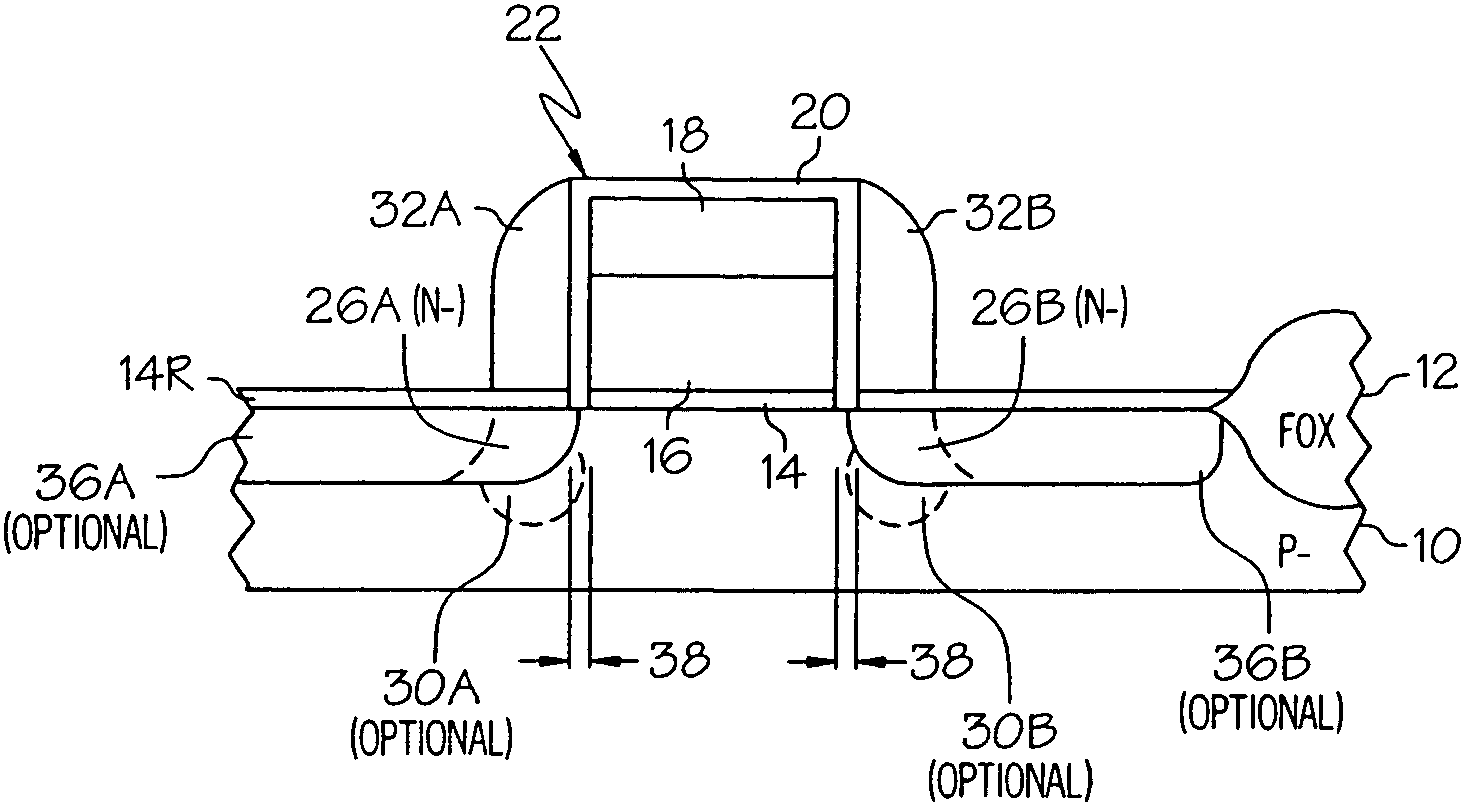
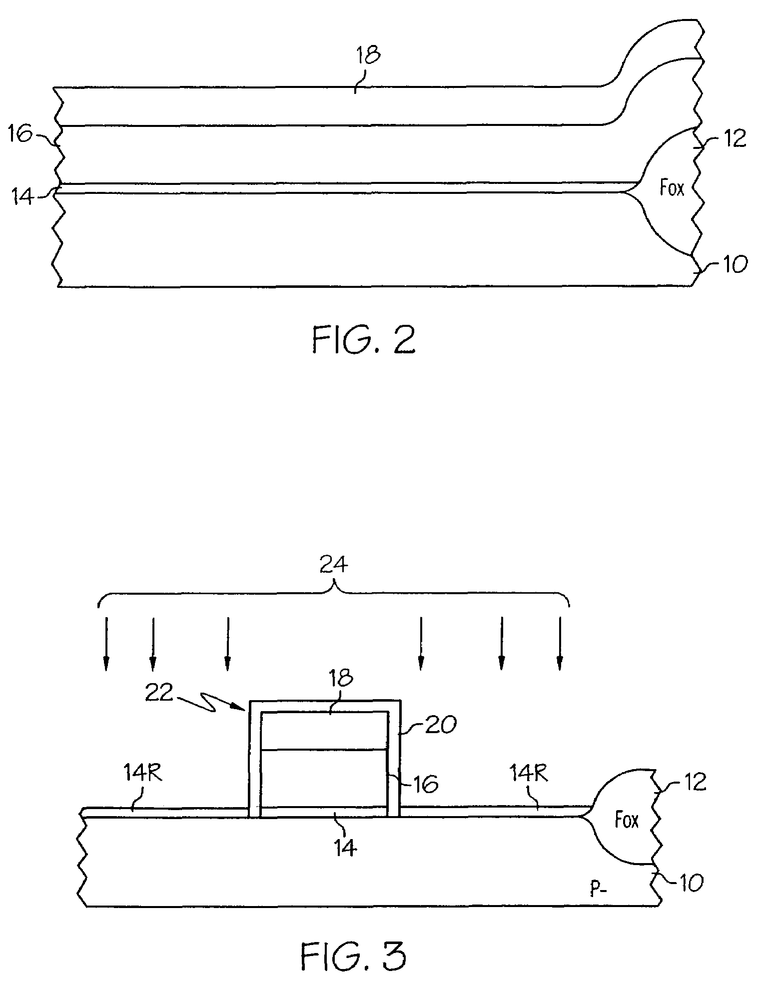
[0033]A sub-micron semiconductor device addressing burn-in reliability and refresh characteristics and methods of fabricating such a device are described. The device includes a MOS transistor having two-layer doped polysilicon plug. In the following description, numerous specific details are set forth such as specific materials, reticle patterns, dimensions, etc. in order to provide a thorough understanding of the present invention. It will be obvious, however, to one skilled in the art that these specific details need not be employed to practice the present invention. In other instances, known materials or methods are not described in detail to avoid unnecessarily obscuring the present invention.

[0034]Additionally, it should be noted that the process steps and structures described below do not form a complete process flow for manufacturing integrated circuits. The present invention can be practiced in conjunction with integrated circuit fabrication techniques currently used in the ...


PUM


Abstract

A method of manufacturing a memory device addressing reliability and refresh characteristics through the use of a multilayered doped conductor, and a method making is described. The multilayered doped conductor creates a high dopant concentration in the active area close to the channel region. The rich dopant layer created by the multilayered doped conductor is less susceptible to depletion from trapped charges in the oxide. This improves device reliability at burn-in and lowers junction leakage, thereby providing a longer period between refresh cycles.

Description

CROSS REFERENCE TO RELATED APPLICATIONS[0001]This application is a division of U.S. patent application Ser. No. 10 / 650,563 filed Aug. 28, 2003 now U.S. Pat. No. 6,858,534, which in turn is a division of U.S. patent application Ser. No. 10 / 230,948 filed Aug. 29, 2002, now U.S. Pat. No. 6,670,682, issued on Dec. 30, 2003.BACKGROUND OF THE INVENTION[0002]The present invention relates to the field of semiconductor memory devices, and more particularly, to a structure having improved burn-in reliability and refresh characteristics in dynamic random access memory (DRAM) devices and a method of making it.[0003]Metal oxide semiconductor (MOS) structures are basic electronic devices used in many integrated circuit (IC) devices. One such structure is the metal oxide semiconductor field effect transistor (MOSFET), which is typically formed in a semiconductor substrate by providing a gate structure over the substrate to define a channel region, and by forming source / drain regions on opposing si...

Claims


Application Information

Patent Timeline
Patent Type & Authority Patents(United States)
IPC IPC(8): H01L21/425H01L21/4763G06Q10/06G06Q30/02H01L21/225H01L21/285H01L21/768H01L21/8242
CPCG06Q10/063G06Q10/0631G06Q10/06311G06Q10/06312G06Q30/0202G06Q30/0205H01L21/26586H01L21/28512H01L21/28525H01L21/76877H01L27/10855H01L27/10888H01L29/6656H01L29/6659H01L2924/0002H01L21/2254H01L21/2257H01L21/823425H01L21/823475H01L23/485H01L27/10873H01L29/1083H01L2924/00H10B12/0335H10B12/05H10B12/485
Inventor MOULI, CHANDRA V.
Owner MICRON TECH INC
Why Eureka
Try Eureka