Transistor, method for producing an integrated circuit and a method of producing a metal silicide layer

a technology of integrated circuits and metal silicide layers, which is applied in the direction of basic electric elements, electrical apparatus, and semiconductor devices. it can solve the problems of inability to implement structures of reduced dimensions, poor power data in respect of finished circuits, and inability to meet the technological demands of conventional silicon technology. achieve the effect of high level of device integration density and simple method implementation

Inactive Publication Date: 2007-03-27
IHP GMBH INNOVATIONS FOR HIGH PERFORMANCE MICROELECTRONICS LEIBNIZ INST FUR INNOVATIVE
View PDF14 Cites 11 Cited by
  • Summary
  • Abstract
  • Description
  • Claims
  • Application Information

AI Technical Summary

Benefits of technology

[0011]The object of the invention is to provide a transistor and a method of producing an integrated circuit, which while invol

Problems solved by technology

At the present time however no satisfactory solutions with which those technological demands can be fulfilled are known in the area of conventional silicon technology.
The implementation of structures of reduced dimensions is not possible with the material SiO2 (silicon oxide, silicon dioxide) used hitherto as the gate oxide, as high tunnel currents occur with the required gate oxide thick

Method used


Image

  • Transistor, method for producing an integrated circuit and a method of producing a metal silicide layer
  • Transistor, method for producing an integrated circuit and a method of producing a metal silicide layer
  • Transistor, method for producing an integrated circuit and a method of producing a metal silicide layer

Examples


Embodiment Construction

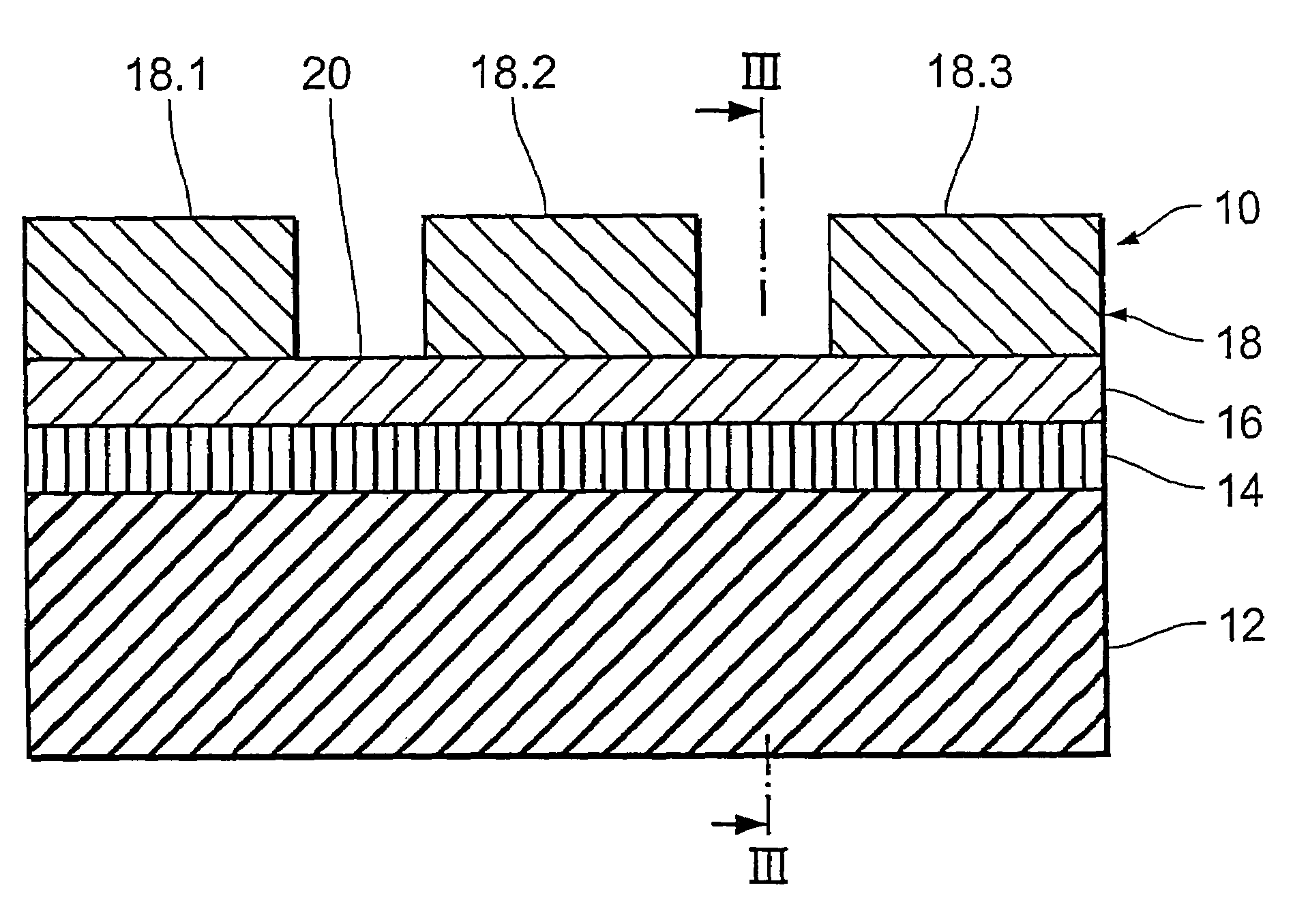
[0064]FIG. 1 shows a simplified view in section through an embodiment of an MOS-transistor 10 during production thereof, more specifically prior to the tempering step in a reducing, oxygen-free gas atmosphere. A silicon wafer 12 is preprepared for integrated CMOS or BiCMOS-circuits and in the region illustrated in FIG. 1 laterally selectively provided with the required implantations for the implementation of an MOS-transistor and its source and drain contacts. Corresponding details which fully correspond to the present state of the art are omitted from FIG. 1 for the sake of simplicity of the drawing.

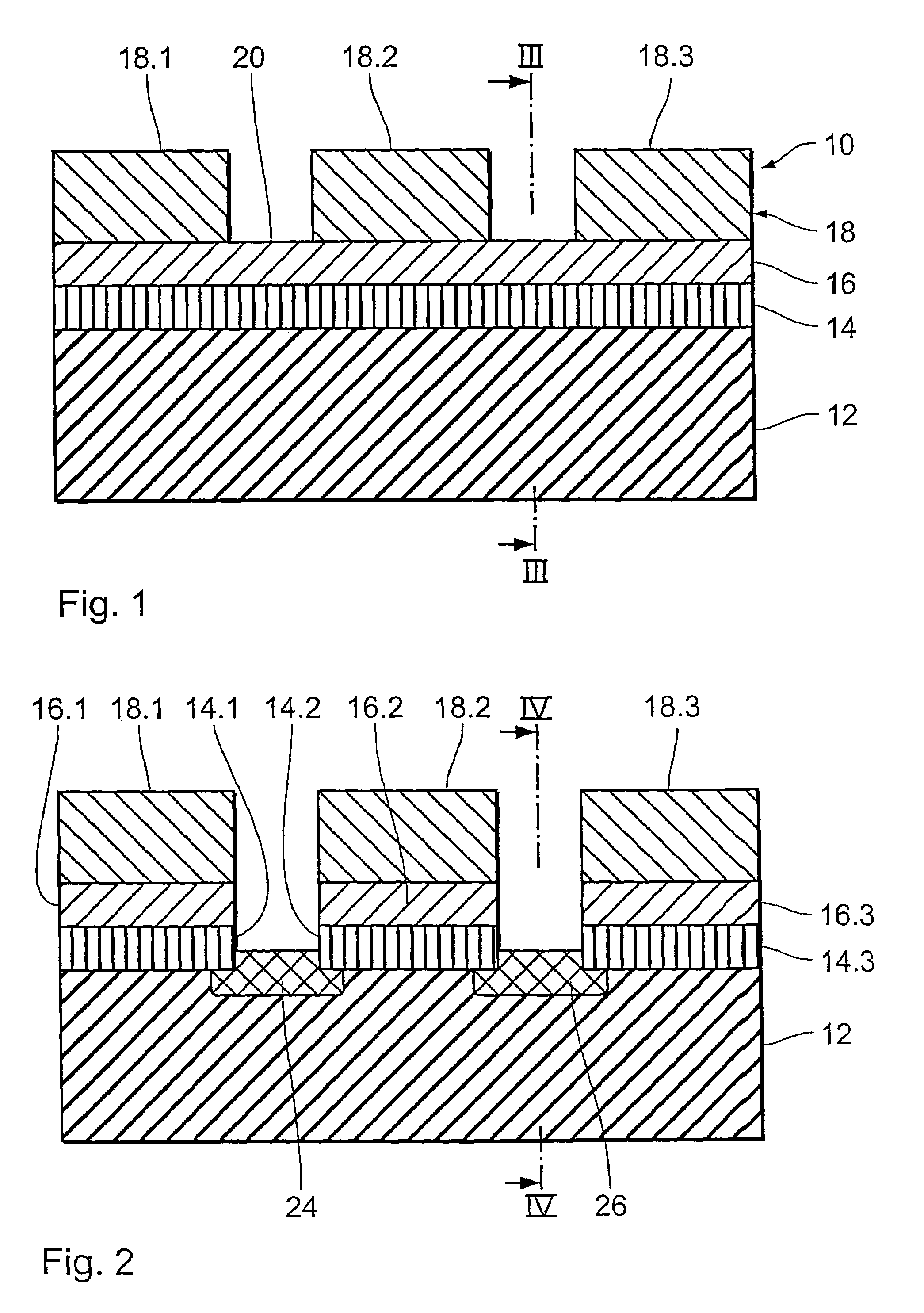
[0065]A praseodymium oxide layer 14 is deposited on the wafer surface. The thickness thereof is uniform in the lateral direction and is between 10 and 30 nanometres. Deposited on the praseodymium oxide layer 14 is a silicon layer 16 whose layer thickness in the lateral direction is also uniform and is between 10 and 30 nanometres. Three cover layer portions 18.1, 18.2, 18.3 of a cover l...


PUM


Abstract

The invention relates to a method for the selective silicidation of contact areas that allow the production of highly integrated circuits, preferably in a SMOS or BiCMOS process. To this end, a metal oxide layer (14) that contains for example praseodymium oxide is deposited onto a prepared wafer (12). A silicon layer (16) and on top of said silicon layer a cover layer (18) is deposited onto the metal oxide layer (14), said cover layer being laterally structured. In a subsequent tempering step in an oxygen-free, reducing gas atmosphere the silicon layer (16) and the metal oxide layer (14) are converted to a metal silicide layer in lateral sections (20, 22) in which the cover layer (18) was previously removed.

Description

CROSS REFERENCE TO RELATED APPLICATIONS[0001]This application is for entry into the U.S. national phase under §371 for International Application No. PCT / EP02 / 05773 having an international filing date of May 24, 2002, and from which priority is claimed, and which in turn claims priority from German patent Application No. DE 101 55 915.1 filed on Nov. 12, 2001, and from German Patent Application No. DE 101 27 234.0 filed on May 26, 2001.TECHNICAL FIELD[0002]The invention concerns a transistor having a metal silicide-bearing contact region between a semiconductor region and a metallically conducting region. The invention further concerns a method of producing an integrated circuit on a substrate, in which a metal silicide-bearing contact region is produced on a silicon surface in one or more lateral portions. Finally the invention concerns a method of producing a metal silicide layer on a substrate with a silicon surface.BACKGROUND OF THE INVENTION[0003]Highly integrated memory and log...

Claims


Application Information

Patent Timeline
IPC IPC(8): H01L29/76H01L21/28H01L21/285H01L21/336H01L29/417H01L29/45H01L29/51
CPCH01L21/28194H01L21/28518H01L29/66575H01L29/456H01L29/517H01L29/41775
Inventor GORYACHKO, ANDRIYKURPS, RAINERLIU, JING PINGOSTEN, HANS-JÖRG
Owner IHP GMBH INNOVATIONS FOR HIGH PERFORMANCE MICROELECTRONICS LEIBNIZ INST FUR INNOVATIVE
Why Eureka
Try Eureka