

Delay circuit with timing adjustment function
a timing adjustment and circuit technology, applied in the field of delay circuits, can solve the problems of inability to maintain locked state, inability to accurately adjust input signals, degradation of sensitivity, etc., and achieve the effect of stable timing adjustment and high accuracy
- Summary
- Abstract
- Description
- Claims
- Application Information
AI Technical Summary
Benefits of technology
Problems solved by technology
Method used
Image

Examples
first embodiment
[0029
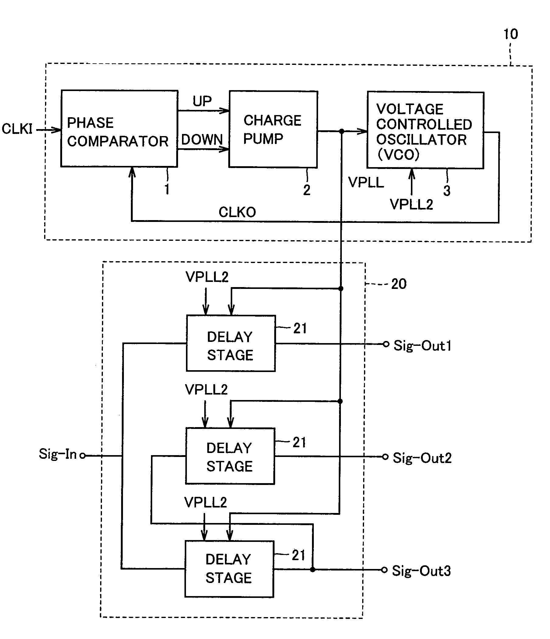
[0030]FIG. 1 is a schematic block diagram showing a configuration of a delay circuit according to a first embodiment of the present invention.
[0031]Referring to FIG. 1, the delay circuit includes a phase locked loop circuit 10 as a clock generating circuit for synchronizing an output clock CLKO with an input clock CLKI to output a control voltage VPLL of voltage controlled oscillator (VCO), and a delay section 20 of which delay time is controlled in response to the supply of control voltage VPLL.
[0032]Phase lock loop circuit 10 includes a phase comparator 1 comparing the phase of input clock CLKI and that of output clock CLKO, a charge pump circuit 2 providing control voltage VPLL in accordance with the result of phase comparison performed by phase comparator 1, and voltage controlled oscillator 3 generating output clock CLKO having the oscillation frequency in accordance with control voltage VPLL.
[0033]Further, output clock CLKO is supplied to an internal circuit (not shown) a...
second embodiment
[0083
[0084]FIG. 6 shows a schematic block diagram of the configuration of a delay circuit according to a second embodiment of the present invention.
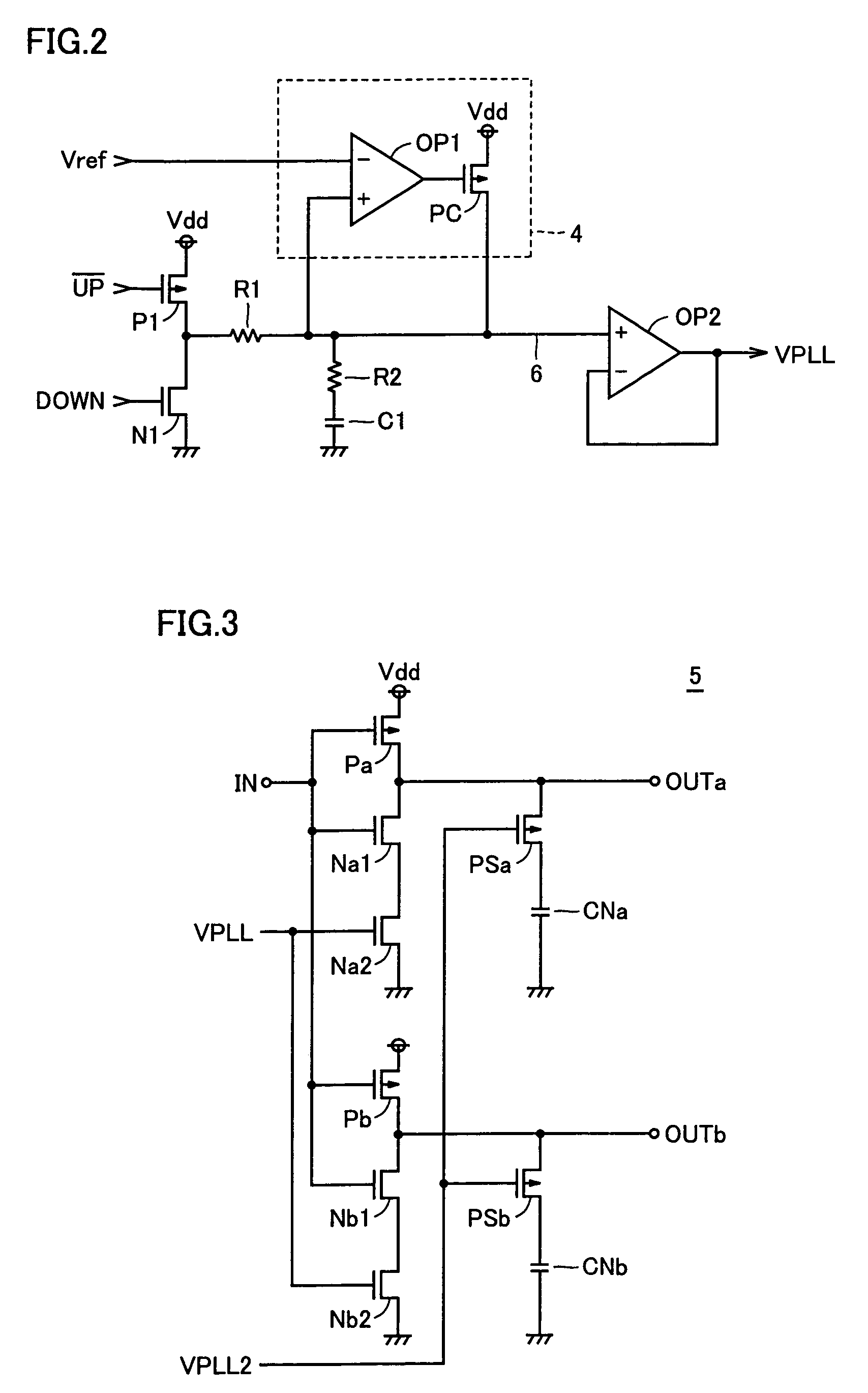
[0085]Referring to FIG. 6, the delay circuit is formed of phase locked loop circuit 10 and a delay section 30. As for phase locked loop circuit 10, since its configuration is similar to that of the delay circuit in the first embodiment shown in FIG. 1, only charge pump circuit 2 is illustrated and the detailed description will not be repeated.
[0086]Delay section 30 includes, as in the first embodiment, a plurality of delay stages 21. In FIG. 6, for simplifying the illustration, only one delay stage is illustrated and the rest of the delay stages are not shown. Delay stage 21 changes the delay time in accordance with a control signal based on control voltage VPLL of charge pump circuit 2, as in the first embodiment.
[0087]Delay section 30 further includes P-channel MOS transistors P2, P3, N-channel MOS transistors N2, N3, and an operationa...
PUM
 Abstract
Description
Claims
Application Information