
Hierarchical method of power supply noise and signal integrity analysis

a power supply and signal integrity analysis technology, applied in error detection/correction, program control, instruments, etc., can solve the problems of significant erroneous at the higher frequencies commonly used today, improper assessment of signal integrity, and difficulty in accurately modeling these electrical phenomena, so as to reduce the number of elements, improve computational efficiency, and accurately simulate

Inactive Publication Date: 2007-03-27
IBM CORP
View PDF2 Cites 9 Cited by
  • Summary
  • Abstract
  • Description
  • Claims
  • Application Information

AI Technical Summary

Benefits of technology

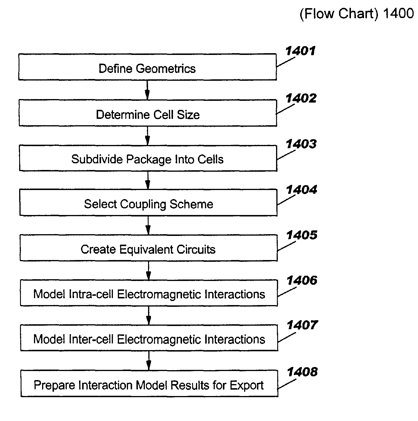
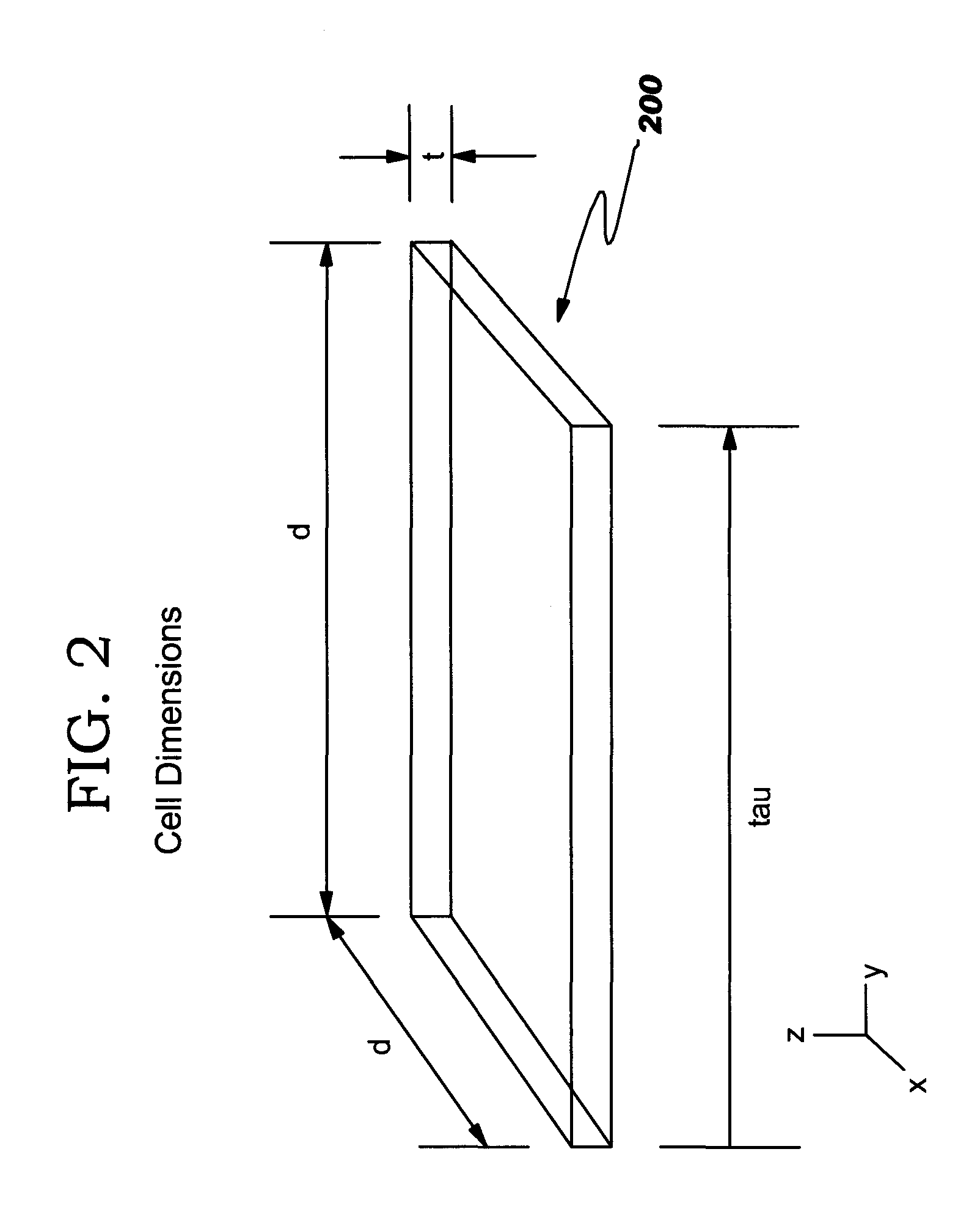
The present invention provides a method for analyzing the electrical interactions in microelectronic packages by dividing the package into smaller cells and modeling the interactions between components using lumped element or field effect coupling techniques. The method takes into account the switching times of signals and the time delays between components. The invention also reduces the number of elements in the model to improve its computational efficiency while retaining the capability of accurately simulating high-speed electromagnetic effects. The invention also provides an electrical circuit signal coupling analysis system for modeling the electrical interactions between functional components of a microelectronic package. The system includes an overall model of the electrical system as a plurality of cells, each cell having at least one directly neighboring cell which is a direct neighbor, wherein each cell has a length, width, and height dimension, and each cell has at least one intra-cell model and one inter-cell model representing the electrical interactions between functional components which are located within the cell. The invention helps to improve the accuracy and efficiency of analyzing the electrical interactions in microelectronic packages.

Problems solved by technology

A long-standing problem in the design of semiconductor integrated circuit chip systems has been the proper assessment of signal integrity, coupling, power supply noise, and resonances such as LC resonance, and package cavity resonance.
Accurately modeling these electrical phenomena is made difficult by the large number of system components—typically at least thousands of vias, hundreds of signal wires, multiple power supplies, and complicated power-plane structures.
The problem is compounded at higher frequencies (i.e., frequency ranges above approximately 1 GHz), where the electromagnetic flight time across the system is longer than the switching time of the signals.
This so-called “lumped element” approach works at low frequencies (e.g., up to about 100 MHz), but yields results that are significantly erroneous at the higher frequencies commonly used today.
However, errors arise with this technique when the rise time of the signals is faster than the interaction of the system's components, which is limited by the speed of light in the medium.
Given a number of signal wires equal to N, the resultant simulation produces an (N×N) matrix, which in turn produces an N-squared computational problem.
As N becomes large, the computations become prohibitively slow.

Method used


Image

  • Hierarchical method of power supply noise and signal integrity analysis
  • Hierarchical method of power supply noise and signal integrity analysis
  • Hierarchical method of power supply noise and signal integrity analysis

Examples


Embodiment Construction

[0045]Although certain embodiments of the present invention will be shown and described in detail, it should be understood that various changes and modifications may be made without departing from the scope of the appended claims. The scope of the present invention will in no way be limited to the number of constituting components, the materials thereof, the shapes thereof, the relative arrangement thereof, etc., and are disclosed simply as an example of an embodiment. The features and advantages of the present invention are illustrated in detail in the accompanying drawings, wherein like reference numerals refer to like elements throughout the drawings.

[0046]The invention described herein provides a method of creating a frequency-dependent electrical model of any electrical system which has a structure that can be modeled as an orthogonal geometric structure. One such electrical system is an integrated chip package which contains horizontal wires, vertical vias, and horizontal cond...


PUM


Abstract

The invention relates generally to a method of power supply noise and signal integrity analysis for creating frequency-dependent electrical models particularly related to microelectronic packages. The method discloses creation of equivalent circuits for geometries encountered in a typical chip package, including how to partition the geometry into cells which are less then 1 / 20 the minimum wavelength (λ) in size, and how to handle signal and power supply vias, signal wires, and power planes. The method also instructs how to assign values to each of the inductors, capacitors, resistors, and transmission lines in each equivalent circuit. The method further provides modeling of only those interactions which occur between adjacent cells.

Description

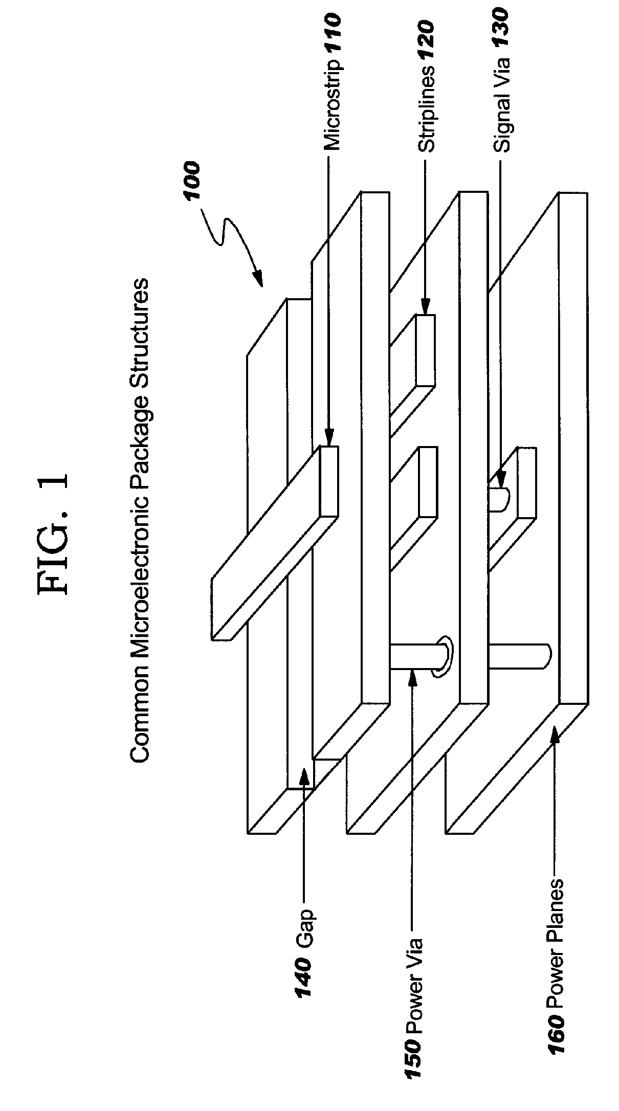
BACKGROUND OF INVENTION[0001]1. Technical Field[0002]The invention relates generally to a method of power supply noise and signal integrity analysis for creating frequency-dependent electrical models, and is particularly related to power supply and signal integrity analysis of microelectronic package structures.[0003]2. Related Art[0004]A long-standing problem in the design of semiconductor integrated circuit chip systems has been the proper assessment of signal integrity, coupling, power supply noise, and resonances such as LC resonance, and package cavity resonance. Accurately modeling these electrical phenomena is made difficult by the large number of system components—typically at least thousands of vias, hundreds of signal wires, multiple power supplies, and complicated power-plane structures. As used throughout this specification, the term “vias” is intended to denote vertical, electrically conductive connections between different electrically conductive planes or signal lines...

Claims


Application Information

Patent Timeline
Patent Type & Authority Patents(United States)
IPC IPC(8): G06F17/50
CPCG06F17/5036G06F2217/78G06F2119/06G06F30/367
Inventor BREILAND, ERIKBUDELL, TIMOTHY W.CHIU, CHARLES S.CLOUSER, PAUL L.ERDELYI, CHARLES K.WELCH, BRIAN P.
Owner IBM CORP
Learn More