Deposition of carbon- and transition metal-containing thin films

a technology of transition metals and thin films, applied in the field of carbon and transition metal-containing thin films, can solve the problems of inability to successfully use transition metal carbides, carbide films, and films likely to contain trace amounts of boron, silicon, or phosphorus contamination, and achieve excellent adhesion and step coverage properties, uniform thickness, and excellent adhesion

Inactive Publication Date: 2007-04-03
BENEQ OY
View PDF17 Cites 13 Cited by
  • Summary
  • Abstract
  • Description
  • Claims
  • Application Information

AI Technical Summary

Benefits of technology

[0014]A process for depositing a carbon- and transition metal-containing thin film on a substrate (hereinafter “the deposition process”) involves placing a substrate within a reaction space, and sequentially pulsing into the reaction space a transition metal chemical and an organometallic chemical (sometimes called a metalorganic chemical). Following each chemical pulse, the reaction space is purged to remove excess chemicals from the reaction space. This pulse and purge sequence is repeated until a desired film thickness is obtained. A preferred deposition process is performed using atomic layer deposition (ALD) techniques and may desirably result in an electrically conductive thin film having uniform thickness over a large substrate area and excellent adhesion and step coverage properties. Further, the resulting film preferably grows at a reasonable growth rate and is chemically inert.

Problems solved by technology

Although ALD has been used in connection with many materials, it has not been successfully used for transition metal carbides.
Due to the chosen carbon sources, the carbide films of the '262 patent are likely to contain trace amounts of boron, silicon, or phosphorus contamination.
Because deposition occurs at high temperatures, the substrate surface layers may be affected by the contaminated carbide film or by boron-, silicon-, or phosphorus-containing carbon source compound in contact with the substrate, which can negatively affect the operability of devices made with the resulting films.
The '262 patent also describes using a hydrocarbon as the carbon source, but states that this alternative carbon source is undesirable because its use involves activation of the reaction with a plasma, requiring a more complicated and expensive reactor design.
Consequently, transition metal carbide films cannot be formed using this method for growing metals.
However, this high temperature treatment decreases the capacity of the process steps and requires the use of expensive and complex manufacturing equipment.

Method used


Image

  • Deposition of carbon- and transition metal-containing thin films
  • Deposition of carbon- and transition metal-containing thin films
  • Deposition of carbon- and transition metal-containing thin films

Examples


example 1a

[0045]A 195 mm×265 mm×1 mm glass substrate and a 200 mm silicon wafer substrate were loaded into the reaction space of a flow-type ALD reactor. The glass substrate was placed on top of a planar substrate holder plate such that only one of the glass substrate surfaces was exposed to the gas flow. The silicon wafer substrate was installed horizontally but supported from the edges in order to keep both sides of the wafer exposed to the gas flow. After loading the substrates into the reactor, the reaction space was pumped down and purged with N2 gas (99.999% purity, AGA Oy). The N2 gas flow rate was adjusted to 3 standard liters per minute (slm) in order to maintain a pressure of about 1 mbar inside the reaction space. The heated reaction space was allowed to stabilize for 5 hours, during which the reaction space and the substrates reached a targeted process temperature of about 400° C.

example 1b

[0046]A 195 mm×265 mm×1 mm glass substrate and a 200 mm silicon wafer substrate were loaded into the reaction space of a flow-type ALD reactor. The glass substrate was placed on top of a planar substrate holder plate such that only one of the glass substrate surfaces was exposed to the gas flow. The silicon wafer substrate was installed horizontally but supported from the edges in order to keep both surfaces of the wafer exposed to the gas flow. After loading the substrates into the reactor, the reaction space was pumped down and purged with N2 gas (99.999% purity, AGA Oy). The N2 gas flow rate was adjusted to 3 standard liters per minute (slm) in order to maintain a pressure of about 1 mbar inside the reaction space. The heated reaction space was allowed to stabilize for 5 hours, during which the reaction space and the substrates reached a targeted process temperature of about 500° C.

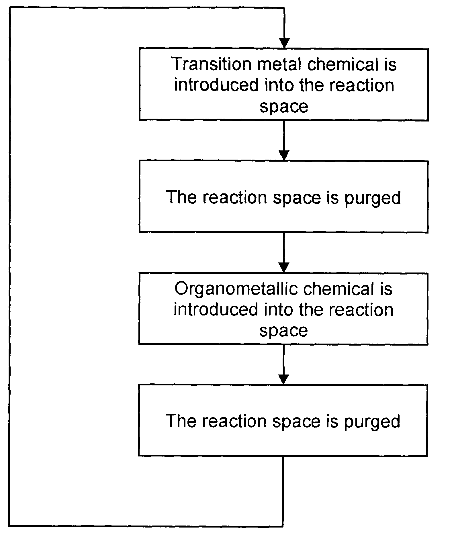
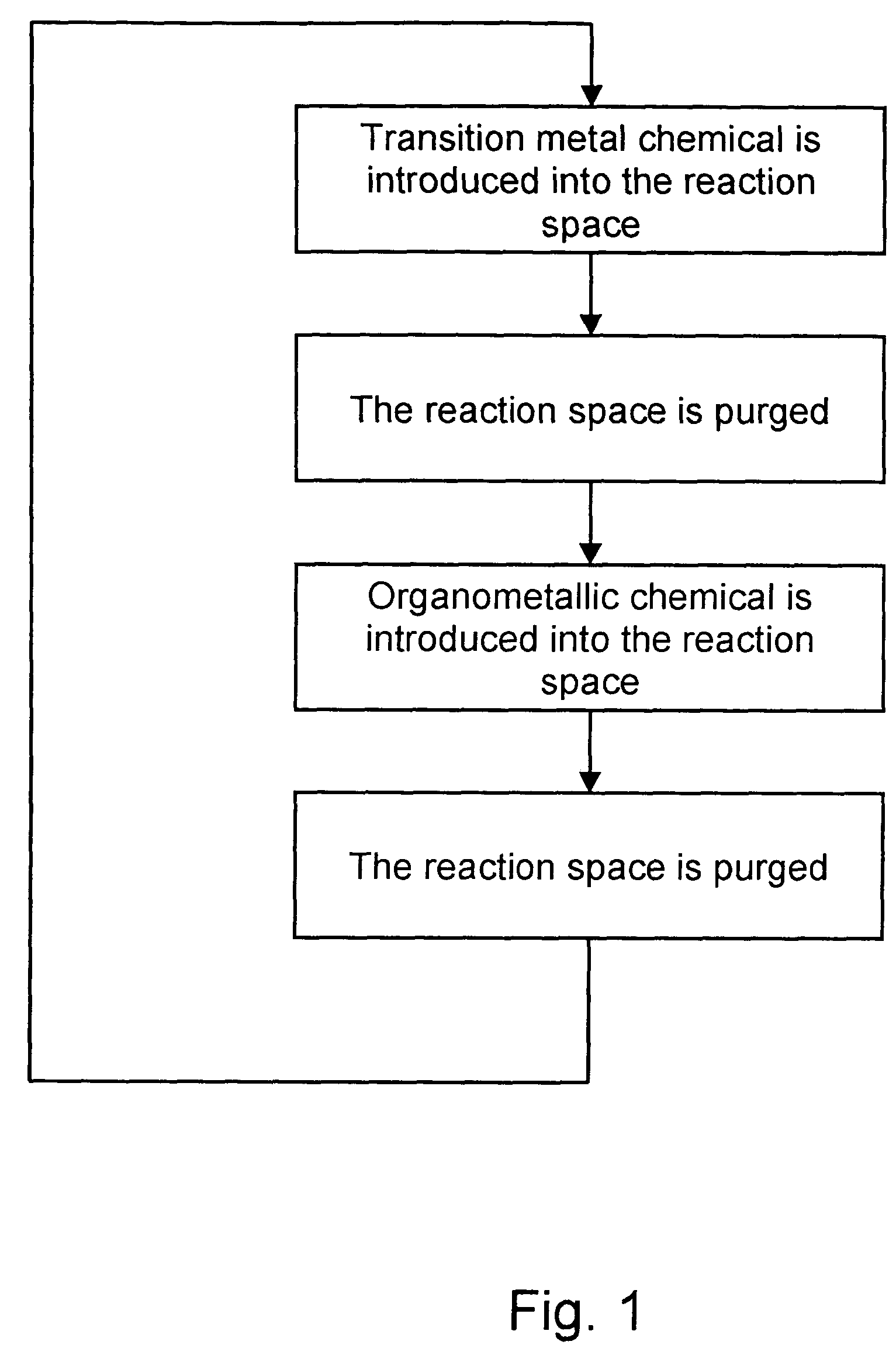
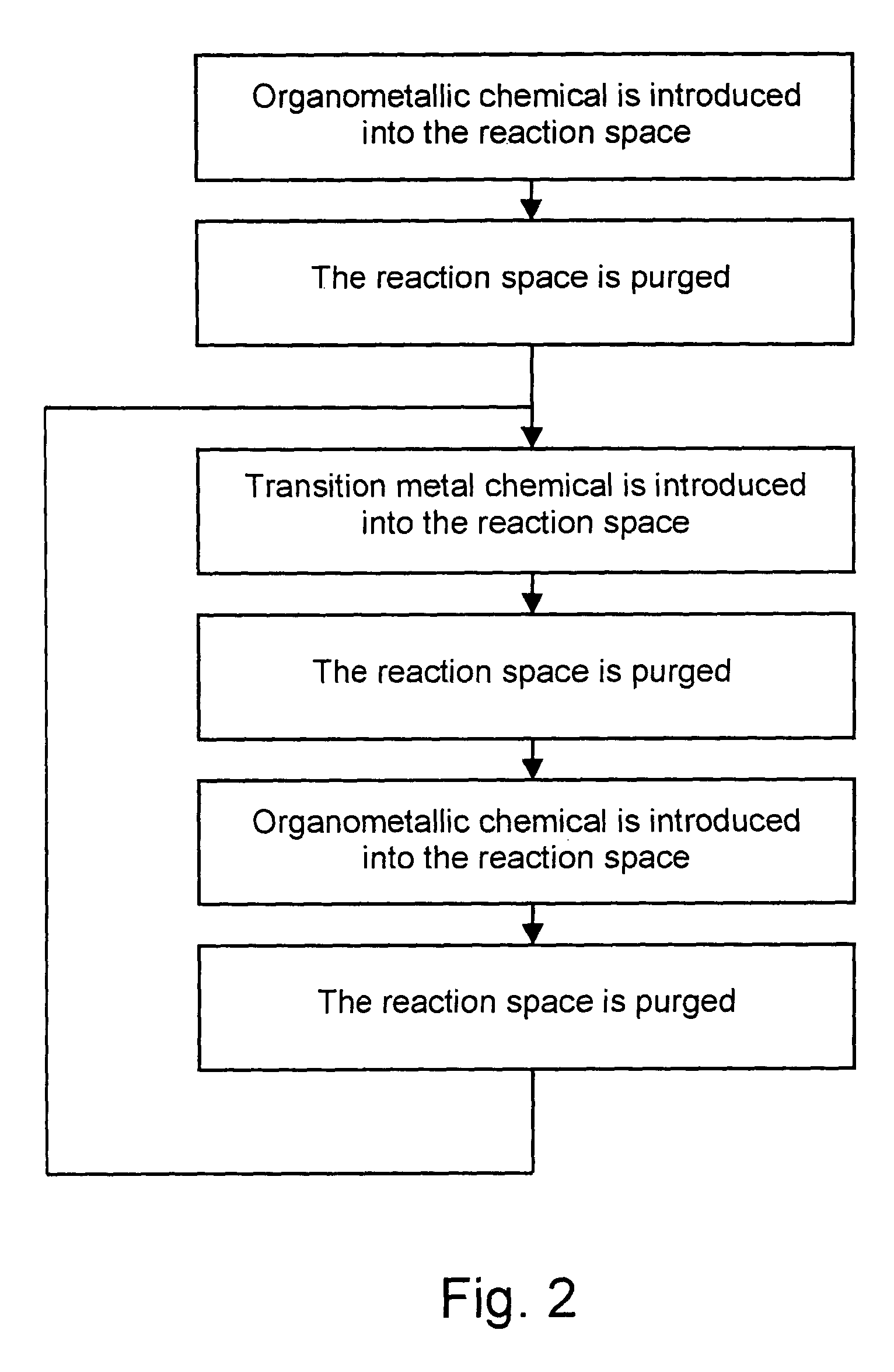
[0047]Alternating pulses of titanium tetrachloride (TiCl4) (99.9% purity, Aldrich), the transition ...

example 2

[0054]A 195 mm×265 mm×1.1 mm glass substrate, a 4 inch silicon wafer substrate, and a 10 mm carbon wafer substrate were loaded into a reaction space of a flow-type ALD reactor. The glass substrate was positioned on top of a planar substrate holder plate in order to expose only one of the glass substrate surfaces to the gas flow. The silicon wafer substrate and the carbon wafer substrate were placed on the glass substrate in order to expose only one surface of each of the wafers to gas flow. After loading the substrates into the reactor, the reaction space was pumped down and purged with N2 gas (99.999% purity, AGA Oy). The N2 gas flow rate was adjusted to 3 slm in order to maintain a pressure of about 1 mbar inside the reaction space. The heated reaction space was allowed to stabilize for 3 hours, during which time the reaction space and substrates reached a temperature of about 525° C.

[0055]Alternating pulses of titanium tetrachloride (TiCl4) (99.9% purity, Aldrich), the transition...


PUM

PropertyMeasurementUnit
pressureaaaaaaaaaa
temperatureaaaaaaaaaa

Abstract

A process depositing a carbon- and transition metal-containing thin film on a substrate involves placing a substrate within a reaction space and sequentially pulsing into the reaction space a transition metal chemical and an organometallic chemical. Following each chemical pulse, the reaction space is purged, and the pulse and purge sequence is repeated until a desired film thickness is obtained. A preferred deposition process uses atomic layer deposition techniques and may result in an electrically conductive thin carbide film having uniform thickness over a large substrate area and excellent adhesion and step coverage properties.

Description

RELATED APPLICATION[0001]This application claims the benefit under 35 U.S.C. § 119(e) of U.S. Provisional Patent Application No. 60 / 445,571, filed Feb. 6, 2003, which is incorporated herein by reference.COPYRIGHT NOTICE[0002]© 2002 Planar Systems, Inc. A portion of the disclosure of this patent document contains material that is subject to copyright protection. The copyright owner has no objection to the facsimile reproduction by anyone of the patent document or the patent disclosure, as it appears in the Patent and Trademark Office patent file or records, but otherwise reserves all copyright rights whatsoever. 37 CFR § 1.71(d).TECHNICAL FIELD[0003]The present invention relates to a process for depositing a thin film including carbon and a transition metal, to films formed by such deposition processes, to structures made with such films, and to devices for forming such films and structures.BACKGROUND OF THE INVENTION[0004]Transition metal carbides are generally known to show a uniqu...

Claims


Application Information

Patent Timeline
Patent Type & Authority Patents(United States)
IPC IPC(8): C23C16/32C23C16/44C23C16/455
CPCC23C16/32C23C16/45527C23C16/4554C23C16/45531Y10T428/12625
Inventor HARKONEN, KARIDOCZY, MARKLANG, TEEMUBAXTER, NATHAN E.
Owner BENEQ OY
Why Eureka
Try Eureka