Semiconductor device with multi-layered wiring arrangement including reinforcing patterns, and production method for manufacturing such semiconductor device

a technology of multi-layered wiring and semiconductor devices, applied in individual semiconductor device testing, semiconductor/solid-state device testing/measurement, instruments, etc., can solve the problems of cracks, cracks, and delay in signal transmission in signal-transmission path, so as to achieve the effect of preventing cracks and peeling in the low-k insulating layer

Inactive Publication Date: 2007-04-03
RENESAS ELECTRONICS CORP
View PDF12 Cites 10 Cited by
  • Summary
  • Abstract
  • Description
  • Claims
  • Application Information

AI Technical Summary

Benefits of technology

[0020]Therefore, an object of the present invention is to provide a semiconductor device with a multi-layered wiring arrangement, including a low-k insulating layer, which is reinforced so that production of cracks and occurrence of peeling in the low-k insulating layer can be effectively prevented.

Problems solved by technology

Since the SOG layer exhibits an inferior adhesion property with respect to both the SiN layer and the SiO2 layer, the SiN layer and the SiO2 layer are liable to be peeled from the SOG layer when being repeatedly subjected to thermal stresses.
In either event, each of the electrode pads is subjected to physical stresses when bonding and connecting either the gold wire or the metal bump thereto, and thus cracks may be produced in the insulating interlayer structures included in the multi-layered wiring arrangement.
Of course, the narrower the signal-transmission path, the larger resistance of the signal-transmission path, resulting in delay of signal transmission in the signal-transmission path.
Of course, the production of the parasitic capacitance results in delay of signal transmission in the signal-transmission paths.
As well known, a low-k insulating layer made of the low-k material exhibits a lower density than that of a silicon dioxide layer, and thus the physical strength of the low-k insulating layer is inferior to that of the silicon dioxide layer.
Also, the low-k insulating layer exhibits an inferior adhesion property with respect to another insulating layer, such as a silicon dioxide layer or the like.
Accordingly, in the production of the multi-layered wiring arrangement, when an insulating interlayer structure is constituted by using the low-k material, cracks are liable to be produced in a low-k insulating layer due to thermal stresses and / or physical stresses.
Also, in the aforesaid damascene process, a chemical and mechanical polishing (CMP) process is involved to polish a copper layer for producing a copper wiring layout pattern, and thus peeling is liable to occur in the low-k insulting layer due to physical stresses produced in the insulating interlayer structures during the CMP process.

Method used


Image

  • Semiconductor device with multi-layered wiring arrangement including reinforcing patterns, and production method for manufacturing such semiconductor device
  • Semiconductor device with multi-layered wiring arrangement including reinforcing patterns, and production method for manufacturing such semiconductor device
  • Semiconductor device with multi-layered wiring arrangement including reinforcing patterns, and production method for manufacturing such semiconductor device

Examples


first embodiment

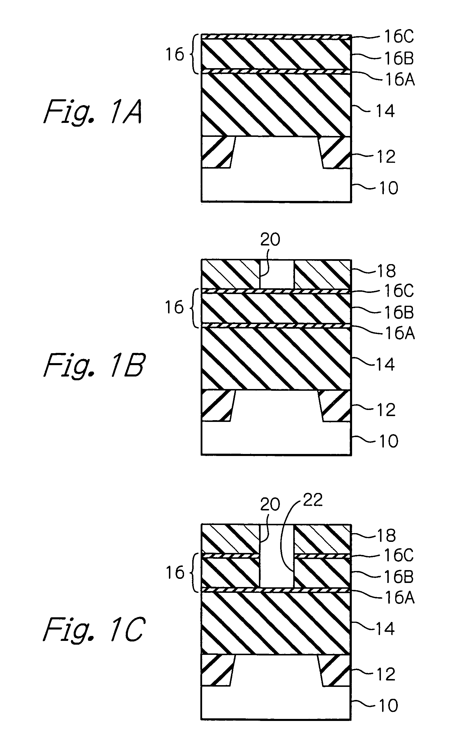
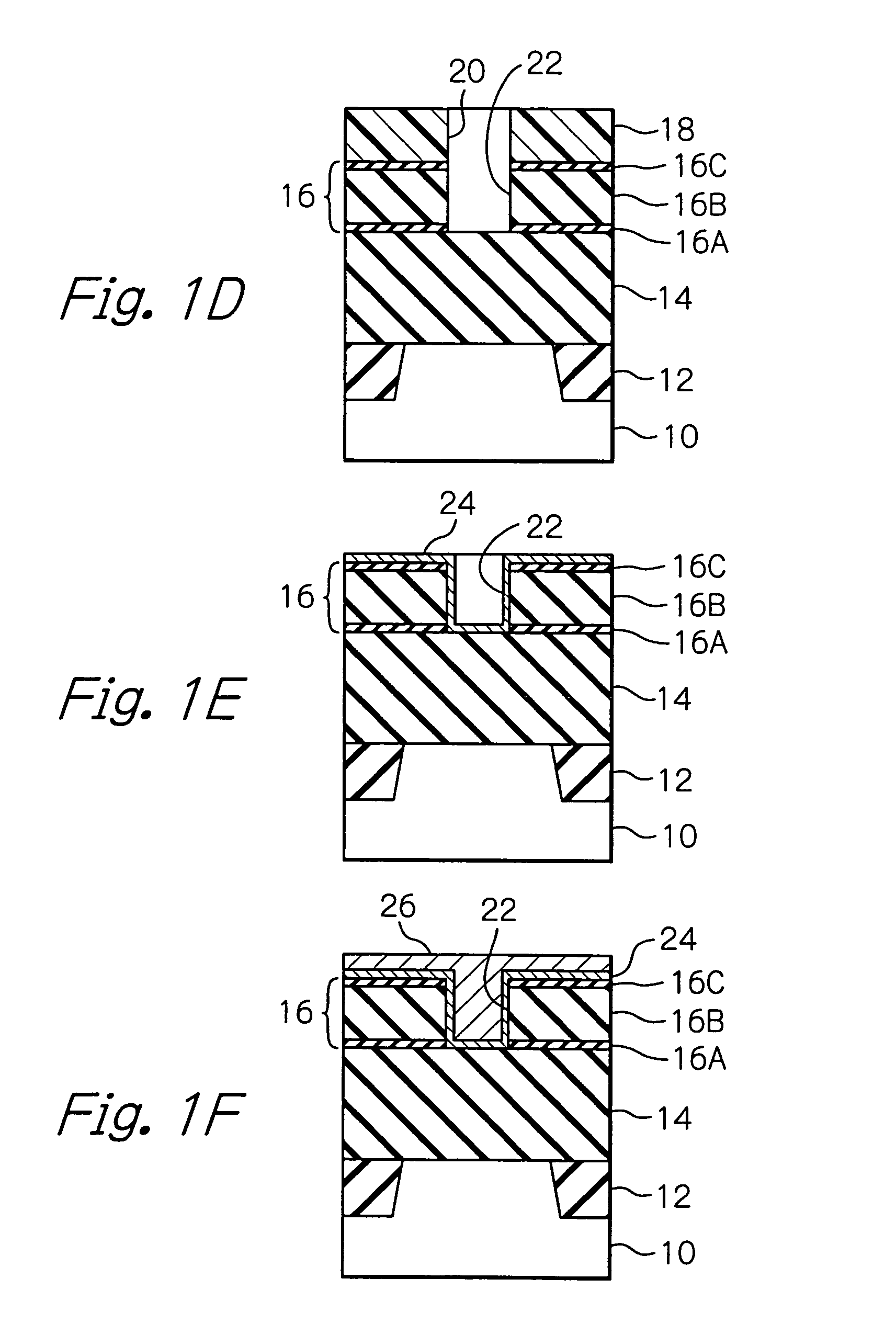
[0074]With reference to FIGS. 1A to 1N, 1P and 1Q, a production method for producing a plurality of semiconductor devices in a silicon wafer, according to the present invention, will be now explained below.

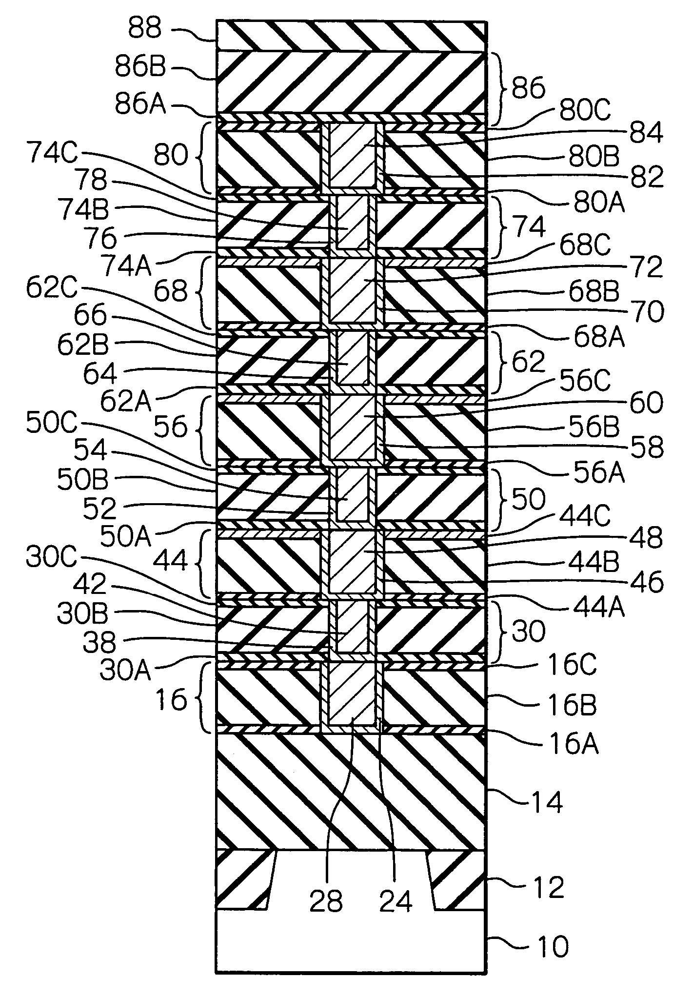
[0075]First, referring to FIG. 1A, a part of a semiconductor substrate 10, defining a semiconductor chip area on a silicon wafer, is illustrated in a vertical cross-sectional view. As shown in this drawing, an element-isolation layer 12 is formed in the semiconductor substrate 10. Note, although not visible in FIG. 1A, various elements, such as transistors, resistors, capacitors and so on, are produced in areas surrounded by the element-isolation layer 12.

[0076]After the production of the various elements is completed, a silicon dioxide layer 14 is formed as an insulating underlayer on the surface of the silicon wafer. Although not visible in FIG. 1A, contact plugs are formed in the insulating underlayer 14, and each of the contact plugs is electrically connected to a correspondin...

second embodiment

[0133]FIG. 5 shows the semiconductor device according to the present invention, and this semiconductor device may be manufactured in substantially the same production method as mentioned above.

[0134]In the second embodiment, the semiconductor device includes a semiconductor substrate 114, which is derived from a silicon wafer. The semiconductor substrate 114 has an element-isolation layer 116 formed therein. Although not visible in FIG. 5, various elements, such as transistors, resistors, capacitors and so on, are produced in areas surrounded by the element-isolation layer 116.

[0135]The semiconductor device also includes a silicon dioxide layer or insulating underlayer 118 formed on the semiconductor substrate 114, and the insulating underlayer 118 has a plurality of tungsten joint plugs formed therein and connected to the semiconductor substrate. Note, in FIG. 5, only one of the joint plugs is indicated by reference 120. Of course, although not visible in FIG. 5, the insulating und...

third embodiment

[0149]FIG. 6A shows the semiconductor device according to the present invention, and this semiconductor device may be manufactured by substantially the same production method as mentioned above.

[0150]In this third embodiment, the semiconductor device includes a semiconductor substrate 146, which is derived from a silicon wafer. The semiconductor substrate 146 has an element-isolation layer 148 formed therein. Although not visible in FIG. 6A, various elements, such as transistors, resistors, capacitors and so on, are produced in areas surrounded by the element-isolation layer 148.

[0151]The semiconductor device also includes a silicon dioxide layer or insulating underlayer 150 formed on the semiconductor substrate 146, and the insulating underlayers 150 includes a plurality of tungsten joint plugs, and a plurality of tungsten contact plugs formed therein. In FIG. 6A, two of the joint plugs are indicated by references 1521 and 1522, and three of the contact plugs are indicated by refer...


PUM


Abstract

A semiconductor device includes a semiconductor substrate having electronic elements produced therein, and an insulating underlayer formed thereon, and a multi-layered wiring arrangement constructed on the insulating underlayer semiconductor substrate. The multi-layered wiring arrangement includes a first insulating interlayer structure formed on the insulating underlayer, a second insulating interlayer structure, and a third insulating interlayer structure formed on the first insulating interlayer structure. Each of the first, second and third insulating interlayer structures includes a low-k insulating layer, and has a reinforcing element formed therein. The second insulating interlayer structure has a joint plug formed therein. The reinforcing elements of the first and third insulating interlayer structures are connected to each other through the joint plug.

Description

BACKGROUND OF THE INVENTION[0001]1. Field of the Invention[0002]The present invention relates to a semiconductor device with a multi-layered wiring arrangement including reinforcing metal patterns formed therein, and a production method for manufacturing such a semiconductor device.[0003]2. Description of the Related Art[0004]In a representative process of producing a plurality of semiconductor devices, for example, a silicon wafer is prepared, and a surface of the silicon wafer is sectioned into a plurality of semiconductor chip areas by forming grid-like fine grooves (i.e. scribe lines) in the silicon wafer. Then, the silicon wafer is processed by various well-known methods such that various elements, such transistors, resistors, capacitors and so on, are produced in each of the semiconductor chip areas on the silicon wafer, and an insulating layer, such as a silicon dioxide layer, is formed as an underlayer on the silicon wafer. Also, a plurality of contact plugs, made of a suita...

Claims


Application Information

Patent Timeline
Patent Type & Authority Patents(United States)
IPC IPC(8): H01L21/4763H01L23/52H01L21/02H01L21/3205H01L21/768H01L23/00H01L23/498H01L23/522H01L23/532
CPCH01L23/522H01L23/53295H01L23/564H01L21/76807H01L21/76832H01L2924/0002H01L2924/00
Inventor OZAWA, KEN
Owner RENESAS ELECTRONICS CORP
Why Eureka
Try Eureka