Nitride semiconductor light emitting device having electrode electrically separated into at least two regions

a light-emitting device and nitride technology, applied in the direction of solid-state devices, semiconductor lasers, lasers, etc., can solve the problems of reducing the yield of self-pulsation, poor stability of active layer and saturable absorption layer, and affecting the performance of the active layer. , to achieve the effect of stable light output and favorable self-pulsation characteristics

Active Publication Date: 2007-04-03
SHARP FUKUYAMA LASER CO LTD
View PDF22 Cites 14 Cited by
  • Summary
  • Abstract
  • Description
  • Claims
  • Application Information

AI Technical Summary

Benefits of technology

[0008]In view of the foregoing, an object of the present invention is to provide a nitride semiconductor light emitting device stable in light output and exhibiting favorable self pulsation characteristics without thermal hysteresis during the growing step.

Problems solved by technology

On occasions where such a nitride semiconductor laser is employed as the light source of an optical disk system and the like, the problem of the reflected light from the disk surface recombining with the semiconductor laser to cause optical feedback noise is of concern.
The aforementioned active layer and saturable absorption layer containing In exhibit poor stability in characteristics due to strain by the substrate and variation in the growing conditions.
It is to be particularly noted that variation in the characteristics of the saturable absorption layer may degrade the yield of self pulsation.
The difference in the growth temperature may sometimes become more than 300° C. Thus, there is a possibility that the processing step during deposition will be rendered complicated by the provision of such a saturable absorption layer.
Also, the thermal hysteresis during deposition may adversely affect the characteristics of the active layer.
It is considered that, for the purpose of obtaining favorable self pulsation, the aforementioned structure is subject to limitation imposed by the material or the structure such as the high differential gain of the active layer, feasible diffusion of carriers, and the like.

Method used


Image

  • Nitride semiconductor light emitting device having electrode electrically separated into at least two regions
  • Nitride semiconductor light emitting device having electrode electrically separated into at least two regions
  • Nitride semiconductor light emitting device having electrode electrically separated into at least two regions

Examples


example 1

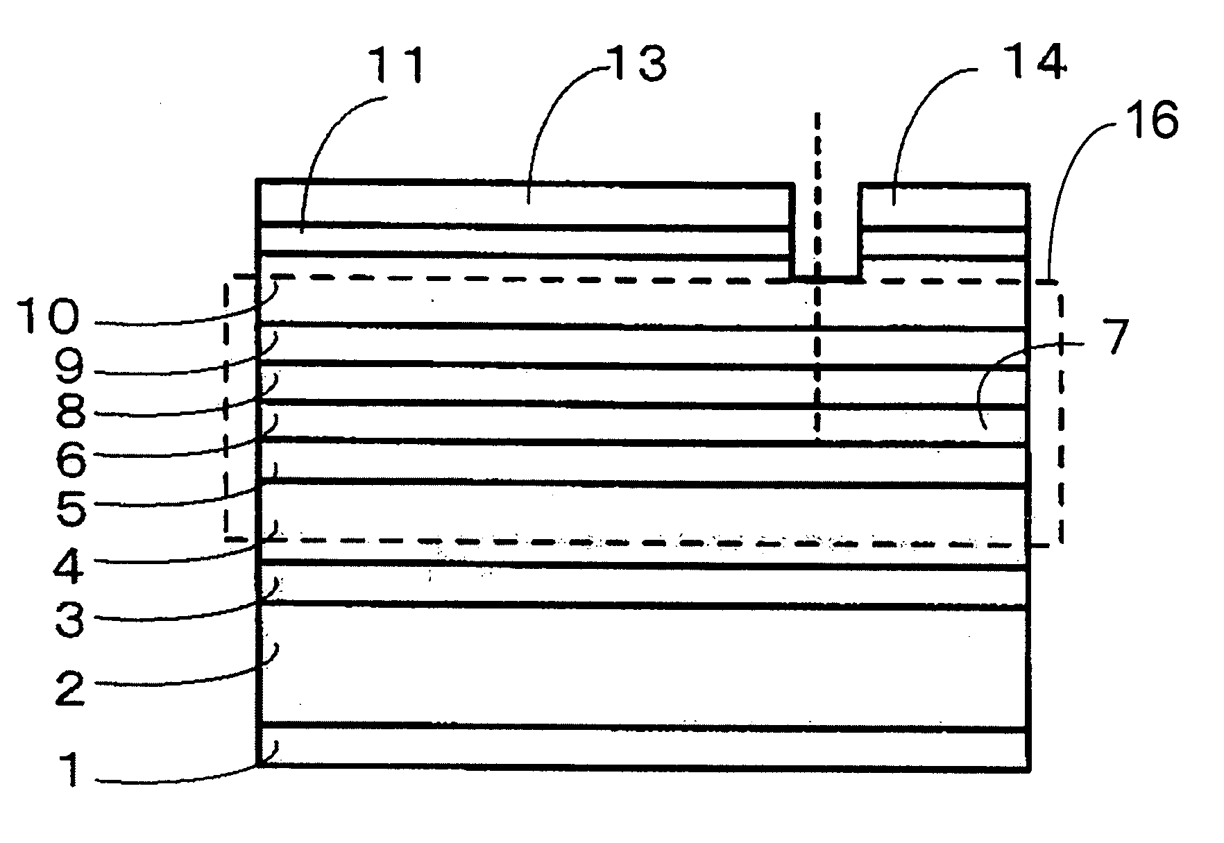
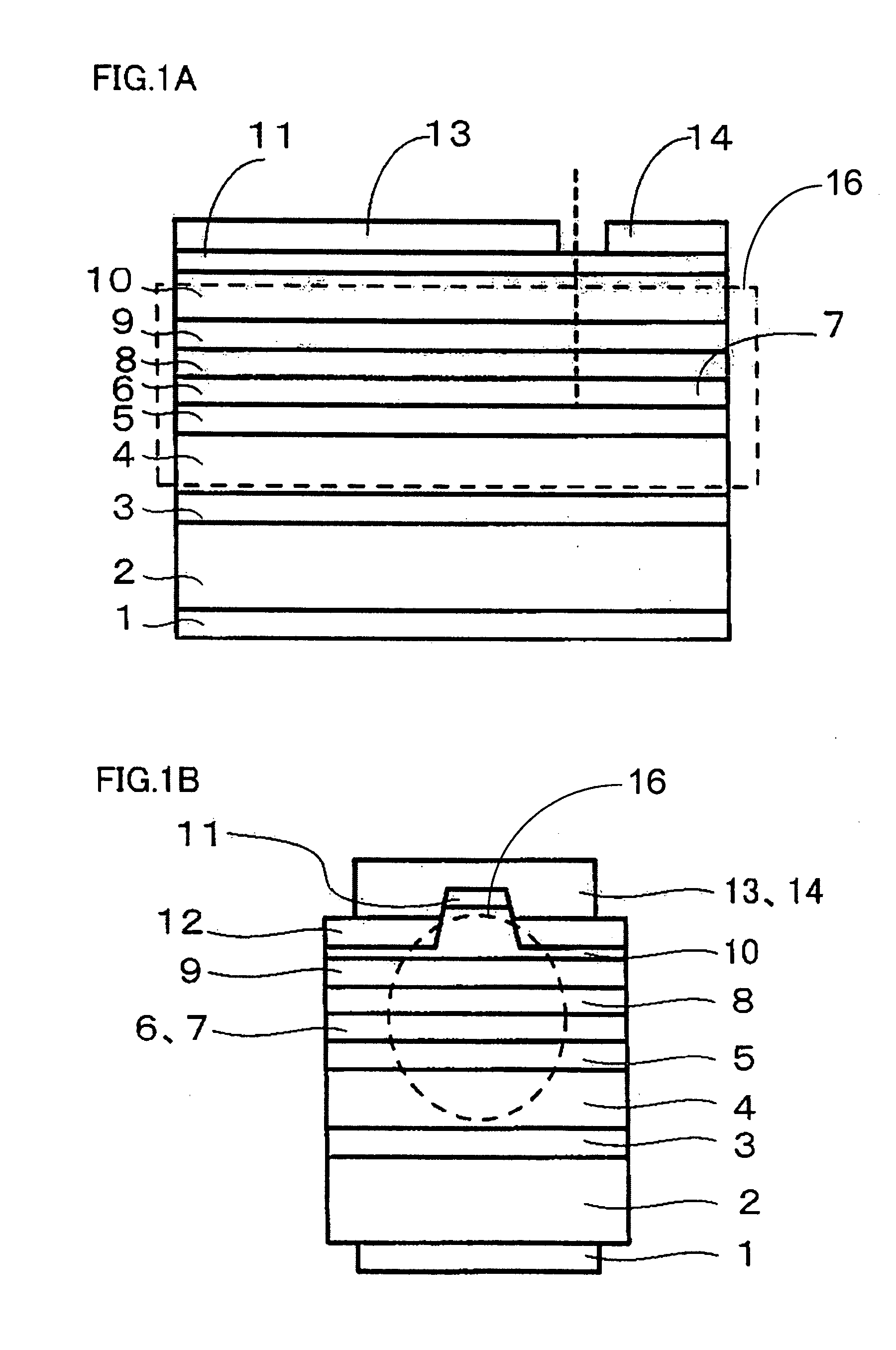
[0070]Example 1 will be described with reference to FIGS. 1A and 1B. FIG. 1A is a vertical sectional view parallel with the cavity of a semiconductor laser device identified as nitride semiconductor light emitting device of the present example, and FIG. 1B is a sectional view vertical with respect to the cavity. From the substrate side are located an n-electrode 1, a GaN substrate 2, an n type GaN layer 3, an n type AlGaN clad layer 4, an n type GaN guide layer 5, an active layer 6 formed of a nitride semiconductor containing mainly In and Ga, a saturable absorber 7 formed of a nitride semiconductor containing mainly In and Ga, a p type AlGaN carrier block layer 8, a p type GaN guide layer 9, a p type AlGaN clad layer 10, a p type GaN contact layer 11, an insulation layer 12, a first p-electrode 13, and a second p-electrode 14.

[0071]Active layer 6 formed of a nitride semiconductor containing mainly In and Ga includes a barrier layer and a well layer, constituting a multiple quantum ...

example 2

[0087]In contrast to the ridge waveguide structure of Example 1, a block structure as shown in FIGS. 8A and 8B is employed in Example 2. FIG. 8A is a vertical sectional view parallel with the cavity of a semiconductor laser device identified as nitride semiconductor light emitting device of the present example. FIG. 8B is a sectional view vertical with respect to the cavity. From the substrate side are located an n-electrode 1, a GaN substrate 2, an n type GaN layer 3, an n type AlGaN clad layer 4, an n type GaN guide layer 5, an active layer 6 formed of a nitride semiconductor containing mainly In and Ga, a saturable absorber 7 formed of a nitride semiconductor containing mainly In and Ga, a p type AlGaN carrier block layer 8, a p type GaN guide layer 9, a p type AlGaN clad layer 10, a p type GaN contact layer 11, a block layer 15, a first p-electrode 13, and a second p-electrode 14. Respective layers were fabricated in a manner similar to that described in Example 1.

[0088]The semi...

example 3

[0089]Example 3 is directed to reduce the cost by conducting the electrical short-circuiting between the second p-electrode and the n-electrode in a more simple manner than in Example 1. A semiconductor laser device identified as nitride semiconductor light emitting device of the present example is shown in FIGS. 9A and 9B. FIG. 9A is a vertical sectional view parallel with the cavity of the semiconductor laser device. FIG. 9B is a sectional view vertical with respect to the cavity. From the substrate side are located an n-electrode 1, a GaN substrate 2, an n type GaN layer 3, an n type AlGaN clad layer 4, an n type GaN guide layer 5, an active layer 6 formed of a nitride semiconductor containing mainly In and Ga, a saturable absorber 7 formed of a nitride semiconductor containing mainly In and Ga, a p type AlGaN carrier block layer 8, a p type GaN guide layer 9, a p type AlGaN clad layer 10, a p type GaN contact layer 11, a first p-electrode 13, a second p-electrode 14, and an Al r...


PUM


Abstract

A nitride semiconductor light emitting device includes at least a substrate, an active layer formed of a nitride semiconductor containing mainly In and Ga, a p-electrode and an n-electrode. At least one of the p-electrode and n-electrode is electrically separated into at least two regions.

Description

BACKGROUND OF THE INVENTION[0001]1. Field of the Invention[0002]The present invention relates to nitride semiconductor light emitting devices. More particularly, the present invention relates to a multielectrode type nitride semiconductor light emitting device having at least one of a p-electrode and an n-electrode electrically separated into at least two regions.[0003]2. Description of the Background Art[0004]A nitride semiconductor laser which is one example of a nitride semiconductor light emitting device has attracted much research efforts to be employed as a light source for an optical disk system in view of the emission wavelength being approximately 400 nm. On occasions where such a nitride semiconductor laser is employed as the light source of an optical disk system and the like, the problem of the reflected light from the disk surface recombining with the semiconductor laser to cause optical feedback noise is of concern. It is generally known that the coherence can be reduc...

Claims


Application Information

Patent Timeline
Patent Type & Authority Patents(United States)
IPC IPC(8): H01L29/10H01L21/00H01L29/22H01S3/097H01L33/32H01L33/38H01S5/042H01S5/06H01S5/065H01S5/323
CPCH01L33/38H01L33/32H01S5/0425H01S5/0602H01S5/0658H01S5/32341H01S5/04252H01S5/04254H01S5/04257
Inventor ONO, TOMOKIITO, SHIGETOSHIOKUMURA, TOSHIYUKIMOURI, HIROKAZUMATSUDA, KYOKOKAWAKAMI, TOSHIYUKIKAMIKAWA, TAKESHITANI, YOSHIHIKO
Owner SHARP FUKUYAMA LASER CO LTD
Why Eureka
Try Eureka