Light emitting device and electronic apparatus

a technology of light-emitting devices and electronic devices, which is applied in the direction of organic semiconductor devices, sustainable manufacturing/processing, final product manufacturing, etc., can solve the problems of easy cracking and heavy, glass substrates and quartz substrates are difficult to be made larger, and cannot help reduce the highest temperature of the process, etc., to achieve the effect of suppressing deterioration

Inactive Publication Date: 2007-05-01
SEMICON ENERGY LAB CO LTD
View PDF64 Cites 119 Cited by
  • Summary
  • Abstract
  • Description
  • Claims
  • Application Information

AI Technical Summary

Benefits of technology

[0014]The present invention is, in light of the above problems, to provide a light emitting device which is capable of suppressing deterioration due to diffusion of impurities such a

Problems solved by technology

At present, although many glass substrates and quartz substrates are utilized, there are defaults of being easily cracked and heavy.
Moreover, the glass substrates and quartz substrates are difficult to be made larger in terms of conducting a mass-production, and these are not suitable for that.
However, since the heat resistance of a plastic film is low, it cannot help lowering the highest temperature of the process.
As a result, at present, a TFT is formed which has not so excellent electric characteristics compared with those formed on the glass substrates.
Therefore, light emitting element having a high performance by utilizing a plastic film have not been realized yet.
However, a substrate comprising a plastic is generally easy to transmit moisture and oxygen through it, and deterioration of a light emitting layer is expedited by these staffs, and therefore, a light emitting device is particularly easy to be short-lived.
However, in the insulating film which comprises silicon nitride and silicon nitride oxide, it is hard to adequately prevent moisture and oxygen from being mixed in the light emitting layer.
Further, in case that film form

Method used


Image

  • Light emitting device and electronic apparatus
  • Light emitting device and electronic apparatus
  • Light emitting device and electronic apparatus

Examples


embodiment 1

[0081]An embodiment of the present invention is described with reference to FIGS. 3A–3D and 4Aa–4D. Here, a method of simultaneously manufacturing a CMOS circuit in which n-channel TFT and p-channel TFT are complementarily combined is described in detail.

[0082]First, the first material layer 101, the second material layer 102, a base insulating film 103 are formed on a substrate 100 and a semiconductor film having a crystalline structure is obtained. Then, the semiconductor film is etched to have a desired shape to form semiconductor layers 104 and 105 separated from one another in an island shape.

[0083]A glass substrate (#1737) is used as the substrate 100.

[0084]For the first material layer 101, it has a characteristic of having a tensile stress within a range of 1 to 1×10¹⁰ (Dyne / cm2) after the filming process or directly before the peeling process. If materials using for the above-mentioned first material layer 101 having a tensile stress within the above-mentioned range, the mat...

embodiment 2

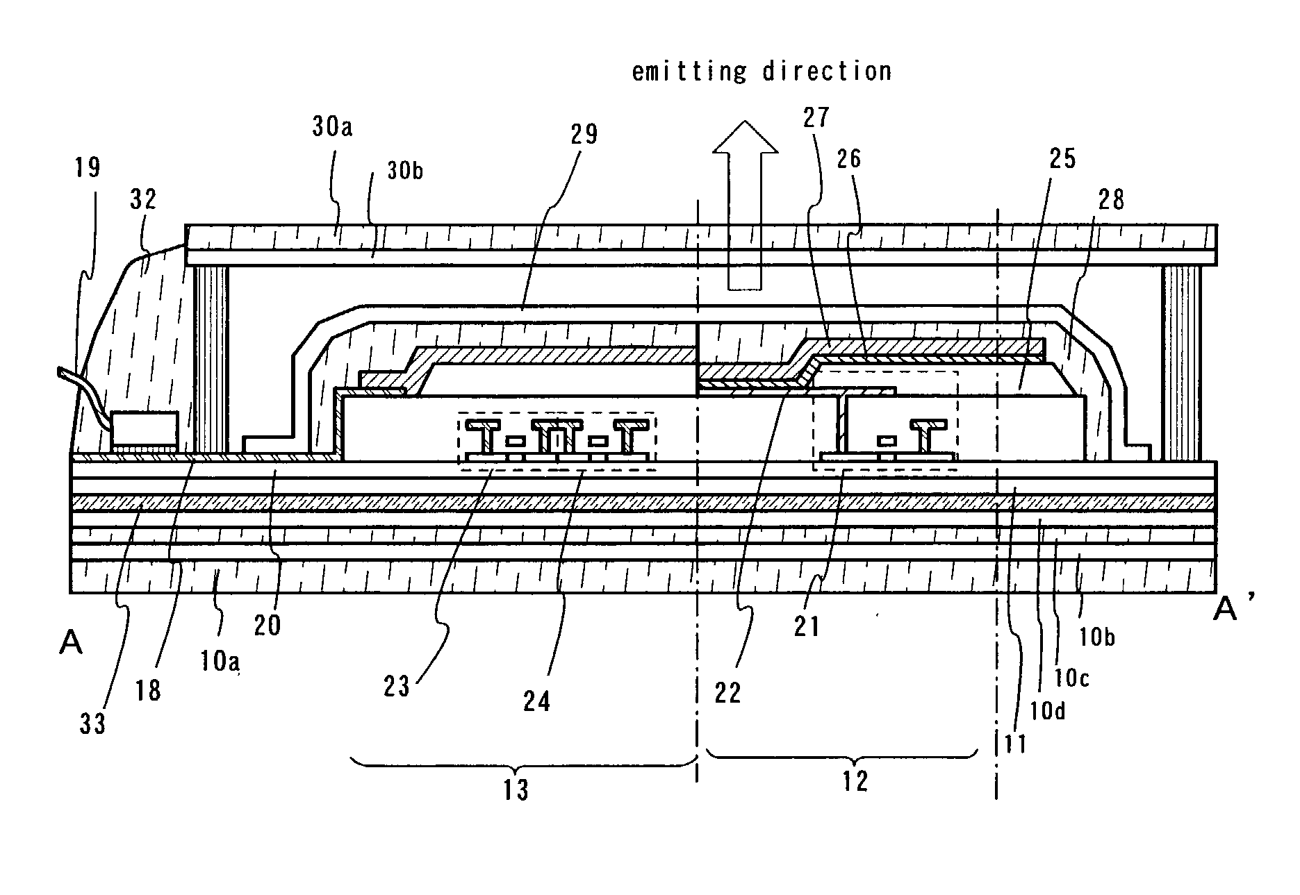
[0112]An example of fabrication of a light emitting device having a light emitting element and using the TFTs obtained in accordance with above Embodiment 1 will be described with reference to FIG. 5.

[0113]FIG. 5 shows an example of a light emitting device (in a state before sealing) having a pixel portion and a drive circuit for driving the pixel portion, the pixel portion and the drive circuit being formed on one insulating member. A CMOS circuit forming a basic unit in the drive circuit and one pixel in the pixel portion are illustrated. The CMOS circuit can be obtained in accordance with Embodiment 1.

[0114]Referring to FIG. 5, a substrate 200, the first material layer 201 and the second material layer 202 are provided. On a base insulating layer 203 formed on the element formation substrate, the drive circuit 204 constituted of an n-channel TFT and a p-channel TFT, a switching TFT, which is a p-channel TFT, and a current control TFT, which is an n-channel TFT, are formed. In thi...

embodiment 3

[0123]Here is shown an embodiment which is different from the process shown in the embodiment 2, and concretely, a peeling process and a bonding process will be described in detail with reference to FIGS. 6A to 6C and 7A and 7B.

[0124]In FIG. 6A, 300 represents a substrate, and 301 represents a nitride layer, and 302 represents an oxide layer, and 303 represents a furring insulating layer, and 304a–304c represent TFTs, and 305 represents a light emitting element, and 306 represents an interlayer insulating film.

[0125]In FIG. 6A, as the substrate 300, a glass substrate, a quartz substrate and a ceramic substrate can be used. Further, a silicon substrate, a metal substrate or a stainless steel substrate may be used.

[0126]Firstly, as shown in FIG. 6A, in accordance with the preferred embodiment, on the substrate 300, a first material layer 301 and a second material layer 302 are formed. It is important to differ film stress of this first material layer 301 from film stress of the second...


PUM


Abstract

A light emitting device which is capable of suppressing deterioration by diffusion of impurities such as moisture, oxygen, alkaline metal and alkaline earth metal, and concretely, a flexible light emitting device which has light emitting element formed on a plastic substrate. On the plastic substrate, disposed are two layers and more of barrier films comprising a layer represented by AlNxOy which is capable of blocking intrusion of moisture and oxygen in a light emitting layer and blocking intrusion of impurities such as an alkaline metal and an alkaline earth metal in an active layer of TFT, and further, a stress relaxation film containing resin is disposed between two layers of barrier films.

Description

BACKGROUND OF THE INVENTION[0001]The present invention relates to a light emitting device, especially, a light emitting device having a light emitting diode formed on a plastic substrate. In addition, it relates to a module using a light emitting diode that mounts IC and the like in which a controller is include in the panel using a light emitting diode. In this specification, the light emitting device is a general term for the panel using a light emitting diode and the module using a light emitting diode. Further, the present invention is related to an electric apparatus using the light emitting device.[0002]In recent years, a technology constituting a thin film transistor (TFT) using a semiconductor thin film (in the range from about a few to a few hundreds nm in thickness) formed on the substrate having an insulating surface has drawn attention. A thin film transistor is widely applied to electronic devices such as an IC, an electro-optic device or the like, and particularly, the...

Claims


Application Information

Patent Timeline
IPC IPC(8): H01L27/15H01L31/12H01L33/00H01L51/52
CPCH01L21/6835H01L51/5253H01L51/0097H01L51/5237H01L51/5256H01L51/529H01L27/3251H01L27/1266H01L29/78603H01L2221/6835H01L2227/326H01L2251/5315H01L2251/5338Y02E10/549H01L27/1214H01L27/1218Y02P70/50H10K77/111H10K50/8426H10K50/8445H10K50/844H10K50/87H10K71/80H10K59/1201H10K2102/3026H10K2102/311H10K59/127
Inventor YAMAZAKI, SHUNPEITAKAYAMA, TORU
Owner SEMICON ENERGY LAB CO LTD
Why Eureka
Try Eureka