Group III nitride semiconductor device

Inactive Publication Date: 2007-05-01
TOYOTA CENT RES & DEV LAB INC
View PDF2 Cites 50 Cited by
  • Summary
  • Abstract
  • Description
  • Claims
  • Application Information

AI Technical Summary

Benefits of technology

[0042]In accordance with the present invention, the voltage resistance of the semiconductor device comprising the group III nitride semiconductor can be increased. Alternatively, the ON resistance of the semiconductor device comprising the group III nitride semi

Problems solved by technology

The presence of the accumulated holes causes dielectric breakdown of the semiconductor device.
In the above-described semiconductor device, this was the factor hindering the realization of increased voltage resistance.
Another problem with such a semiconductor device is rather hi

Method used


Image

  • Group III nitride semiconductor device
  • Group III nitride semiconductor device
  • Group III nitride semiconductor device

Examples


first embodiment

(First Embodiment)

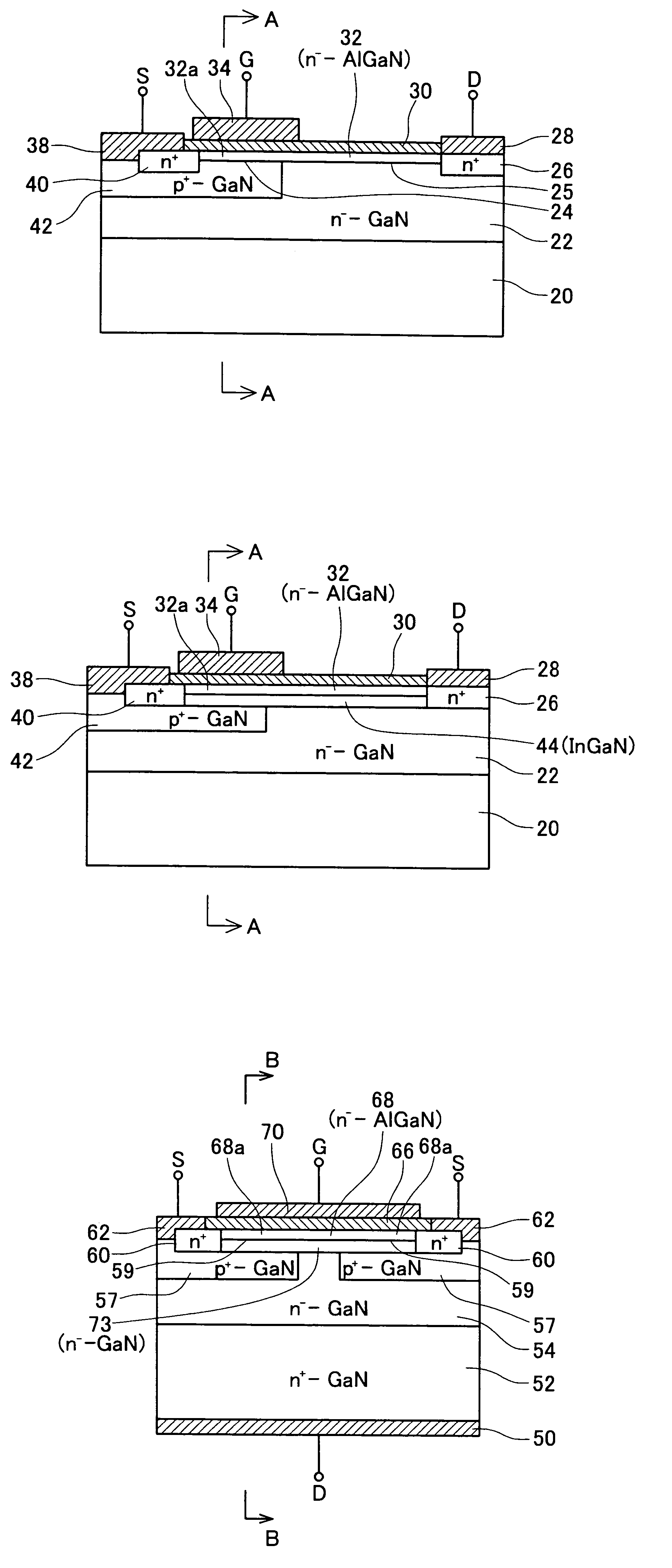
[0060]FIG. 1 is a cross sectional view of a field-effect transistor of the first embodiment. In this transistor, a lower n−-type layer (fourth layer) 22 is formed on a substrate 20. The substrate 20 is composed of Al2O3 (sapphire). The lower n−-type layer 22 is composed of GaN (gallium nitride) doped with Si (silicon), which is an n-type dopant. The concentration of carriers in the lower n−-type layer 22 is about 1×1016 cm−3. The thickness of the thickest portion of the lower n−-type layer 22 is about 5 μm. A p+-type layer (second layer) 42 is formed on the region, which is part of the lower n−-type layer 22. The p+-type layer 42 is composed of GaN doped with Mg (magnesium which is a p-type dopant). The concentration of carriers in the p+-type layer 42 is about 1×1018 cm−3. The thickness of the thickest portion of the p+-type layer 42 is about 0.5 μm. Ge (germanium) or the like may be also doped as the n-type dopant. Be (beryllium) or the like may also be doped as ...

second embodiment

(Second Embodiment)

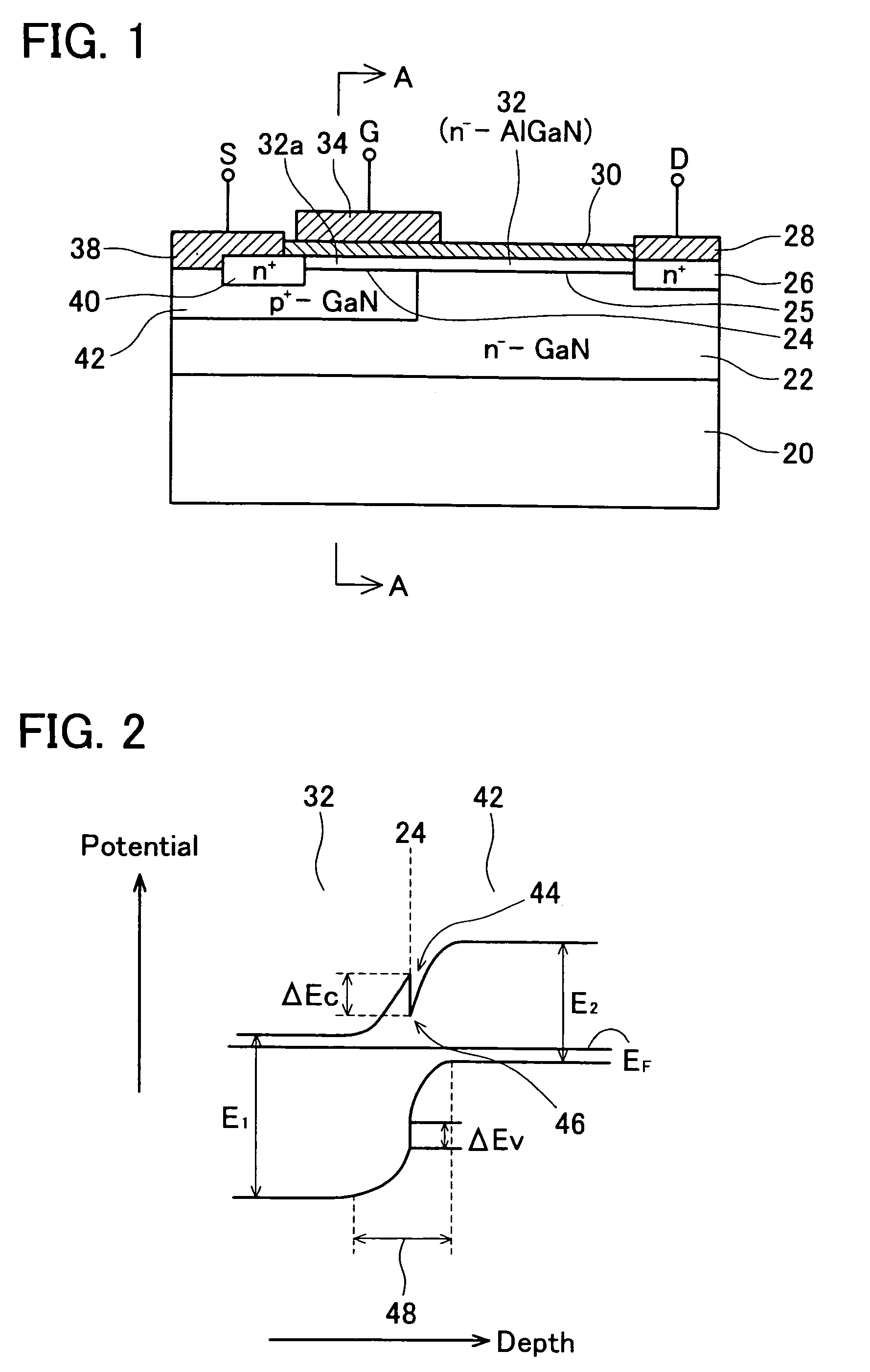
[0081]The field-effect transistor of the second embodiment shown in FIG. 5 is different from that of the first embodiment mainly in the aspects as follows. In the second embodiment, a channel layer (third layer)44 is provided between the upper n−-type layer 32 and the p+-type layer 42. The channel layer 44 is also continuously provided between the upper n−-type layer 32 and the lower n−-type layer 22. The channel layer 44 is composed of true InGaN that was not doped with dopant. Indium is introduced in the channel layer 44. As a result, the band gap of the channel layer 44 is made smaller than the band gaps of the upper n−-type layer 32 and the p+-type layer 42.

[0082]In the second embodiment, the fabrication can be conducted by removing the first mask layer by virtue of a process similar to that of the first embodiment, then successively growing the channel layer 44 and the upper n−-type layer 32 by the MOCVD method over the entire lower n−-type layer 22 and p+-ty...

third embodiment

(Third Embodiment)

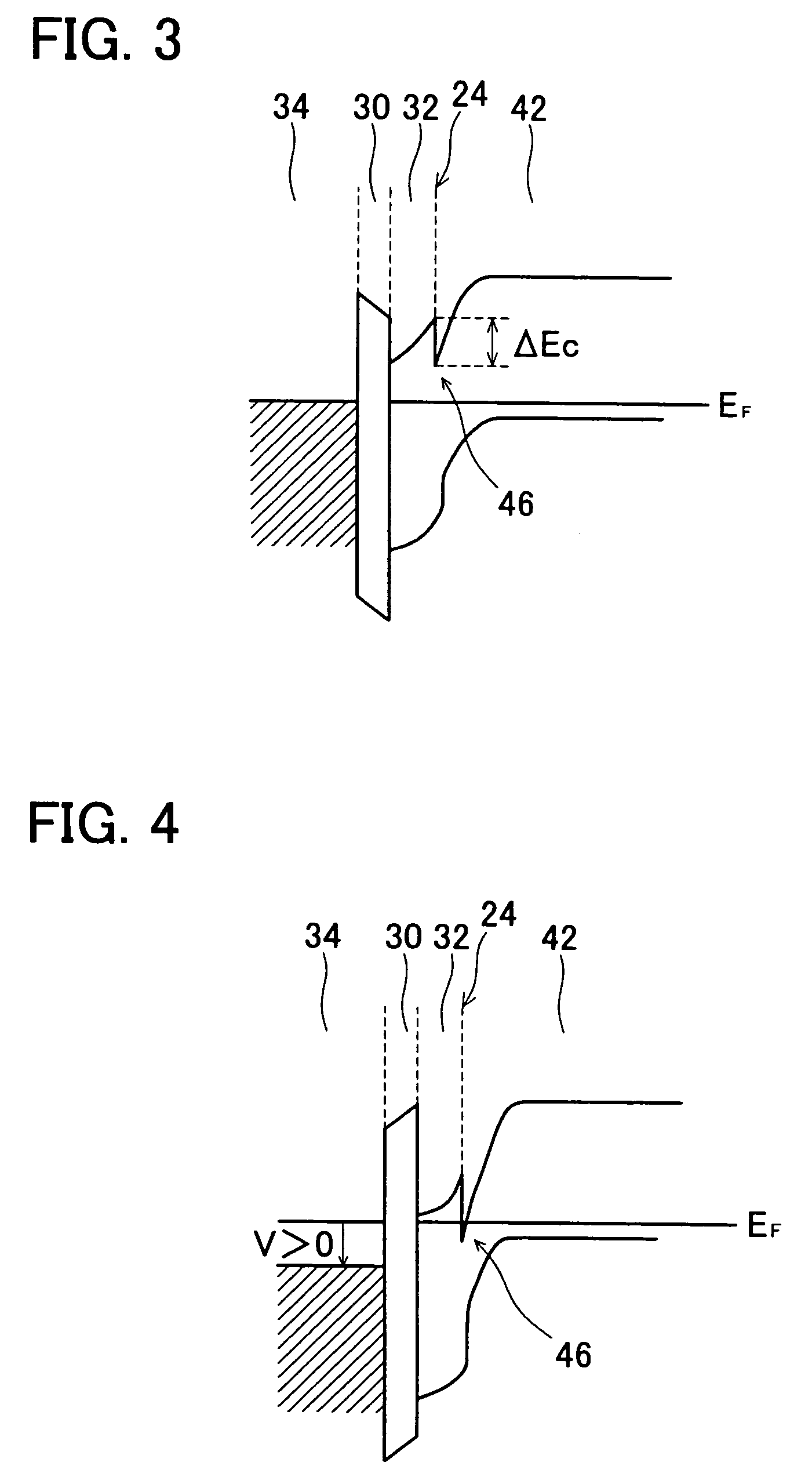
[0085]The field-effect transistor of the third embodiment shown in FIG. 7 has a left-right symmetrical structure of a longitudinal transistor in which a source electrode is formed on the front surface (first surface) of the device and a drain electrode is formed on the rear surface (second surface) of the device. A lower n−-type layer (part of the fourth layer) 54 is formed on an n+-type drain layer (part of the fourth layer) 52. The n+-type drain layer 52 and the lower n−-type layer 54 are composed of GaN that was doped with Si as an n-type dopant. However, the n+-type drain layer 52 was doped with Si to a higher concentration than the lower n−-type layer 54. The concentration of carriers in the n+-type drain layer 52 is about 3×1018 cm−3. The concentration of carriers in the lower n−-type layer 54 is about 1×1016 cm−3. The thickness of the n+-type drain layer 52 is about 200 μm. The thickness of the thickest portion of the lower n−-type layer 54 is about 6 μm. A ...


PUM


Abstract

A semiconductor device is formed by a first layer 32 composed of AlGaN, a second layer 42 composed of GaN, a gate electrode 34, a source electrode 38, and a drain electrode 28. The first layer 32 has a region 32a formed between the gate electrode 34 and the second layer 42. A channel is formed in the vicinity of the boundary 24 of the first layer 32 and the second layer 42. The second layer 42 has p-type conductivity and is in contact with the source electrode 38.
When electrons flow in the channel, the electrons collide with surrounding atoms, and holes are formed. If holes are accumulated inside the semiconductor device, the presence of the accumulated holes causes dielectric breakdown. In the semiconductor device of the invention, holes are discharged to the outside of the device thorough the second layer 42 and the source electrode 38, and accumulation of holes can be prevented.

Description

CROSS-REFERENCE TO RELATED APPLICATIONS[0001]The present application claims priority on Japanese Patent application 2004-003368 filed on Jan. 8, 2004 which claims priority on Japanese Patent application 2003-029374 filed on Feb. 6, 2003, the contents of these applications are hereby incorporated by reference within this specification.[0002]1. Field of the Invention[0003]The present invention relates to a semiconductor device comprising a group III nitride semiconductor.[0004]2. Description of the Related Art[0005]Japanese unexamined patent application publication No. 10-223901 discloses a semiconductor device comprising a group III nitride semiconductor. More specifically, it discloses a field-effect transistor in which a buffer layer, a channel layer, and a gate-insulating layer are stacked successively on a substrate, and a gate electrode is formed thereupon. The channel layer is composed of an n-type GaN (gallium nitride, a group III nitride semiconductor).[0006]When the above-de...

Claims


Application Information

Patent Timeline
IPC IPC(8): H01L29/739H01L29/78H01L21/00H01L29/12H01L29/20H01L29/778
CPCH01L29/7786H01L29/7788H01L29/7789H01L29/2003H01L29/7828H01L29/0646
Inventor KACHI, TETSUNAKANO, YOSHITAKAUESUGI, TSUTOMU
Owner TOYOTA CENT RES & DEV LAB INC
Why Eureka
Try Eureka