Inductive element and manufacturing method of the same

a manufacturing method and technology of inductive elements, applied in the field of inductive elements, can solve the problems of increasing the number of manufacturing stages, unable to manufacture inductive elements with narrow tolerances, and unable to realize high inductance values, etc., to achieve easy mass production, reduce the shift of conductor patterns, and high q characteristic

Active Publication Date: 2007-05-01
TDK CORPARATION
View PDF19 Cites 18 Cited by
  • Summary
  • Abstract
  • Description
  • Claims
  • Application Information

AI Technical Summary

Benefits of technology

[0013]The present invention has been made to solve the above-described problems of the conventional inductive elements, and therefore, has an object to provide an inductive element and a method for manufacturing such an inductive element which can be easily mass-produced, and by which an inductance value of narrow tolerance can be obtained, while a shift in conductor patterns can be reduced. Also, the present invention owns another object to provide an inductive element capable of achieving a high Q characteristic and a method of manufacturing the inductive element having the high Q characteristic.

Problems solved by technology

Also, since the spiral coils are formed on the same planes of the core substrate, very fine processing is highly required for the conductor patterns, so that higher inductance values can be hardly realized.
Therefore, there is such a problem that a total number of manufacturing stages is increased.
Thus, such an inductive element having narrow tolerance can be hardly manufactured.
Furthermore, because the sintered conductor patterns form a coil, it is difficult to obtain a high Q-factor.
Also, there is another problem that such through holes having the well-matched shapes can be hardly formed.

Method used


Image

  • Inductive element and manufacturing method of the same
  • Inductive element and manufacturing method of the same
  • Inductive element and manufacturing method of the same

Examples


first embodiment

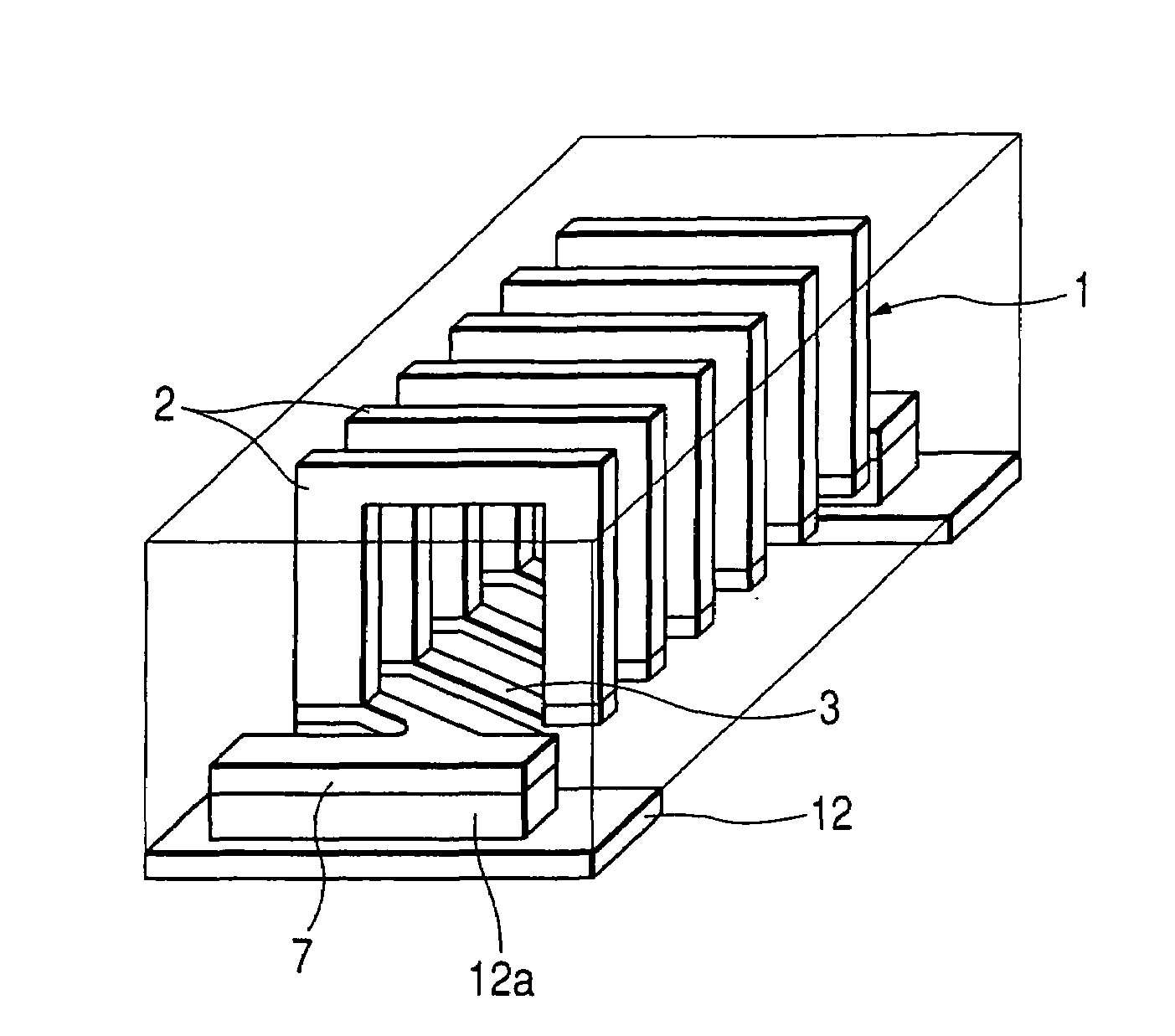
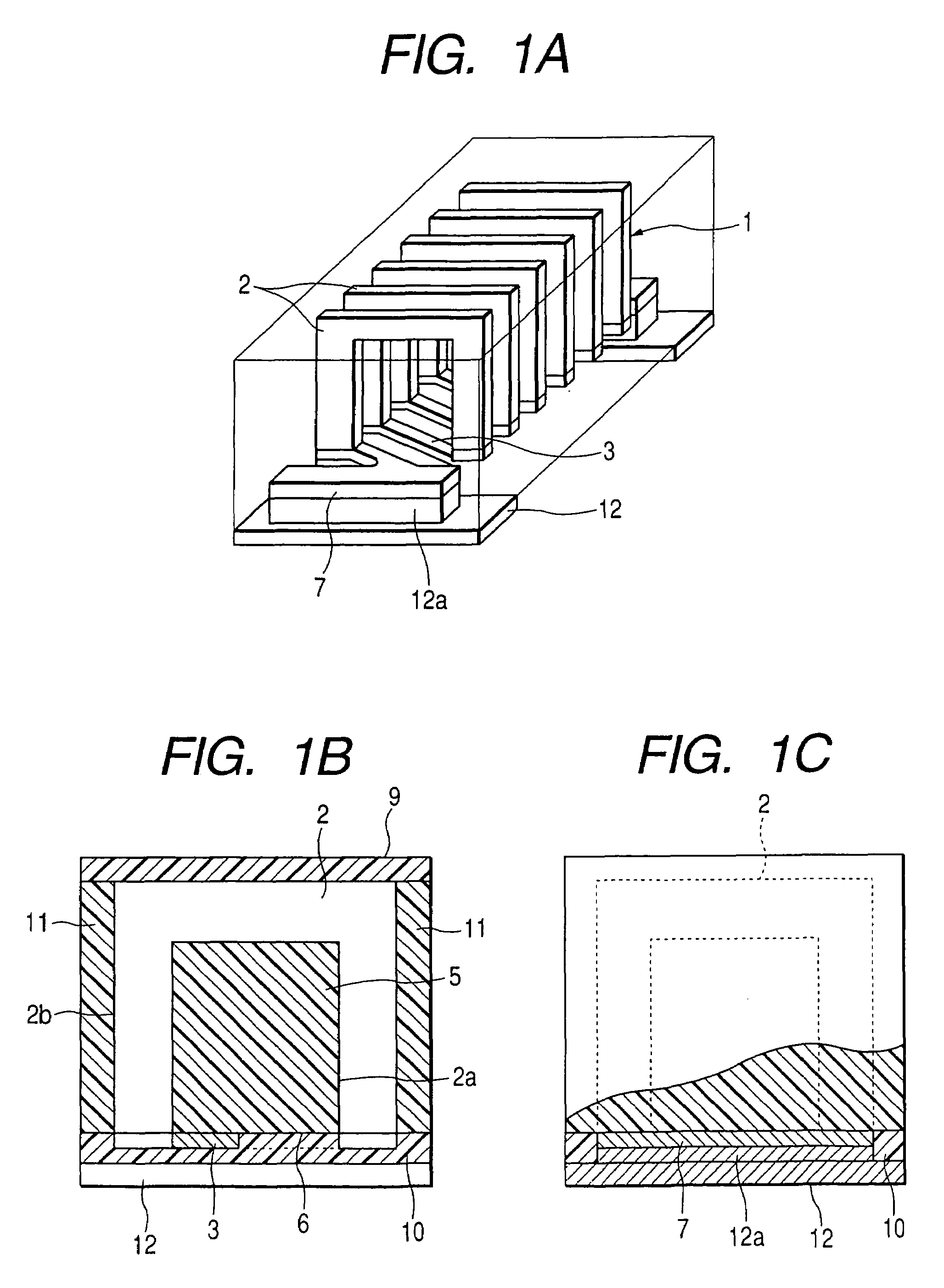
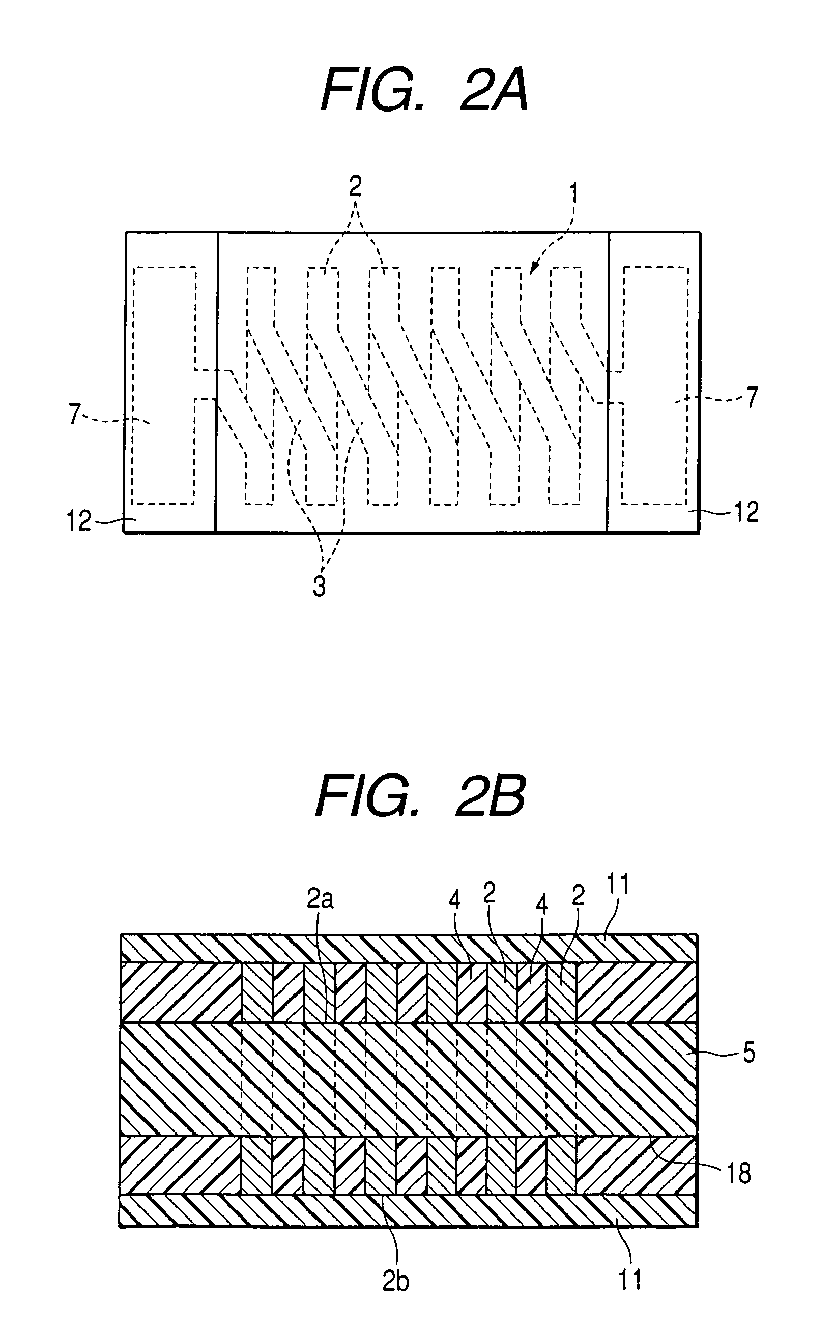
[0085]FIG. 1A is a transparent perspective view for showing an inductive element of a first embodiment of the present invention, FIG. 1B is a sectional view for representing a structure of the inductive element and FIG. 1C is a sectional view for showing an electrode structure of the inductive element. FIG. 2A is a bottom view for showing the inductive element according to this embodiment, and FIG. 2B is a sectional view for representing the inductive element.

[0086]In FIG. 1 and FIG. 2, reference numeral 1 shows a coil which is constructed in a rectangular helical shape. This helical-shaped coil 1 is arranged by a plurality of U-shaped conductors 2 which constitute 3 sides selected from 4 sides of this coil 1, and a bridge conductor 3. The bridge conductor 3 constitutes the remaining 1 side within the four sides, and connects two sets of U-shaped conductors 2 located adjacent to each other so as to constitute the rectangular helical-shaped coil 1 as an entire structure. As indicated...


PUM

PropertyMeasurementUnit
depthaaaaaaaaaa
diameteraaaaaaaaaa
thicknessaaaaaaaaaa

Abstract

Conductor layers 2A and insulating layers 4A are alternately stacked so as to prepare a base material 17. A plurality of grooves 18 having a predetermined width are formed in a surface of the base material 17 in such a manner that these plural grooves 18 are located parallel to each other along a stacking layer direction in order to form a coil inner peripheral portion. Embedding materials 5 are filled into the grooves 18. Surfaces 16 of the base material into which the embedding materials 5 have been filled are flattened by polishing. The conductor layers 2A located adjacent to each other are connected to each other, so that helical coils which constitute inductive elements are constructed. Then, both the front plane and the rear plane of the resultant base material are covered by an insulating layer, which is cut so as to obtain respective chips.

Description

BACKGROUND OF THE INVENTION[0001]The present invention is related to an inductive element and a method of manufacturing the inductive element which is used as an inductor device having a stacked layer structure, a common mode choke coil, or a transformer. Otherwise, this inductive element may be constituted in combination with other elements, or may be used in such a mode that this inductive element is assembled in a module.[0002]As one example of conventional inductive elements, spiral-shaped coils are formed by using a photolithography method on both a front surface and a rear surface of a core substrate, while the core substrate is made of either resin or a composite material manufactured by mixing functional material powder with resin (see, for example, Japanese Patent No. 2714343 (Particularly, pages 3 to 4, FIGS. 3 and 5).[0003]Also, as another prior art, a stacked layer ceramics chip inductor is typically known. That is, since plural layers of green seats having conductor pat...

Claims


Application Information

Patent Timeline
Patent Type & Authority Patents(United States)
IPC IPC(8): H01F5/00H01F41/04H01F17/00H01F17/02
CPCH01F17/0033H01F2017/004H01F5/00
Inventor SATO, SHINICHIOHKUBO, HITOSHIKIKUCHI
Owner TDK CORPARATION
Why Eureka
Try Eureka