Method for fabricating embedded thin film resistors of printed circuit board

a printed circuit board and embedded technology, applied in the field of printed circuit boards, can solve the problems of difficult to achieve constant and precise resistances of resistors, high price, and easy high temperature exposure of printed circuit board lamination, and achieve the effect of reducing the size of the circuit, reducing the risk of failure, and improving the quality of the printed circuit board

Inactive Publication Date: 2007-05-08
SU SUNG LING
View PDF2 Cites 26 Cited by
  • Summary
  • Abstract
  • Description
  • Claims
  • Application Information

AI Technical Summary

Benefits of technology

[0007]The embedded thin film resistors made by the present invention replace the bulky conventional discrete resistors. The printed circuit board can therefore have finer circuit layout and much smaller size. The capacitive reactance effect usually found at the connectors of conventional discrete resistors is also avoided. The signal transmission speed and quality of the printed circuit board is therefore significantly enhanced, especially for high frequency applications. The process for forming the resistor layer provided by the present invention is very similar to that used for ordinary printed circuit boards and can be carried out using the same equipment. Therefore there is no significant investment on new equipment. The process for forming the resistor layer provided by the present invention, just like the process for ordinary printed circuit boards, is applicable in mass production and contributes to a significant lower manufacturing cost.

Problems solved by technology

However, because the laminate of the printed circuit board is susceptible to high temperature, low curing temperature carbon paste is usually used.
Therefore, resistors having constant and precise resistances are difficult to achieve.
However, because the nickel-plated copper foil is difficult to manufacture, there are only limited supply sources and therefore the price is high.
Although there are methods using the electroless deposition technology, the fabricated thin film resistors have inadequate adherence due to certain process factors.
The application of these methods for mass production is thereby limited.

Method used


Image

  • Method for fabricating embedded thin film resistors of printed circuit board
  • Method for fabricating embedded thin film resistors of printed circuit board
  • Method for fabricating embedded thin film resistors of printed circuit board

Examples


first embodiment

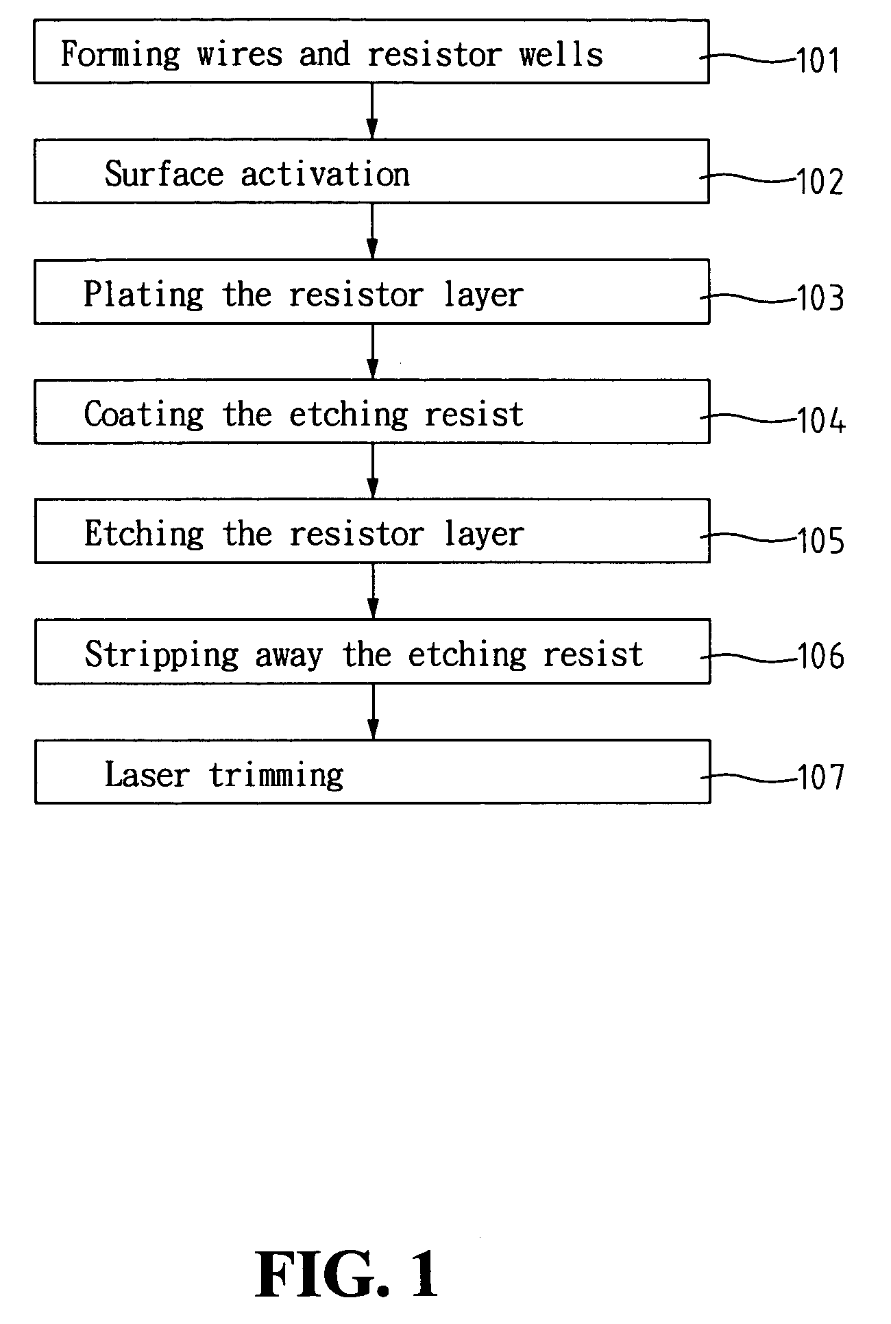
[0014]FIG. 1 is a flow chart showing the steps of forming embedded thin film resistors on a printed circuit board according to the present invention. These steps are described sequentially as follows.

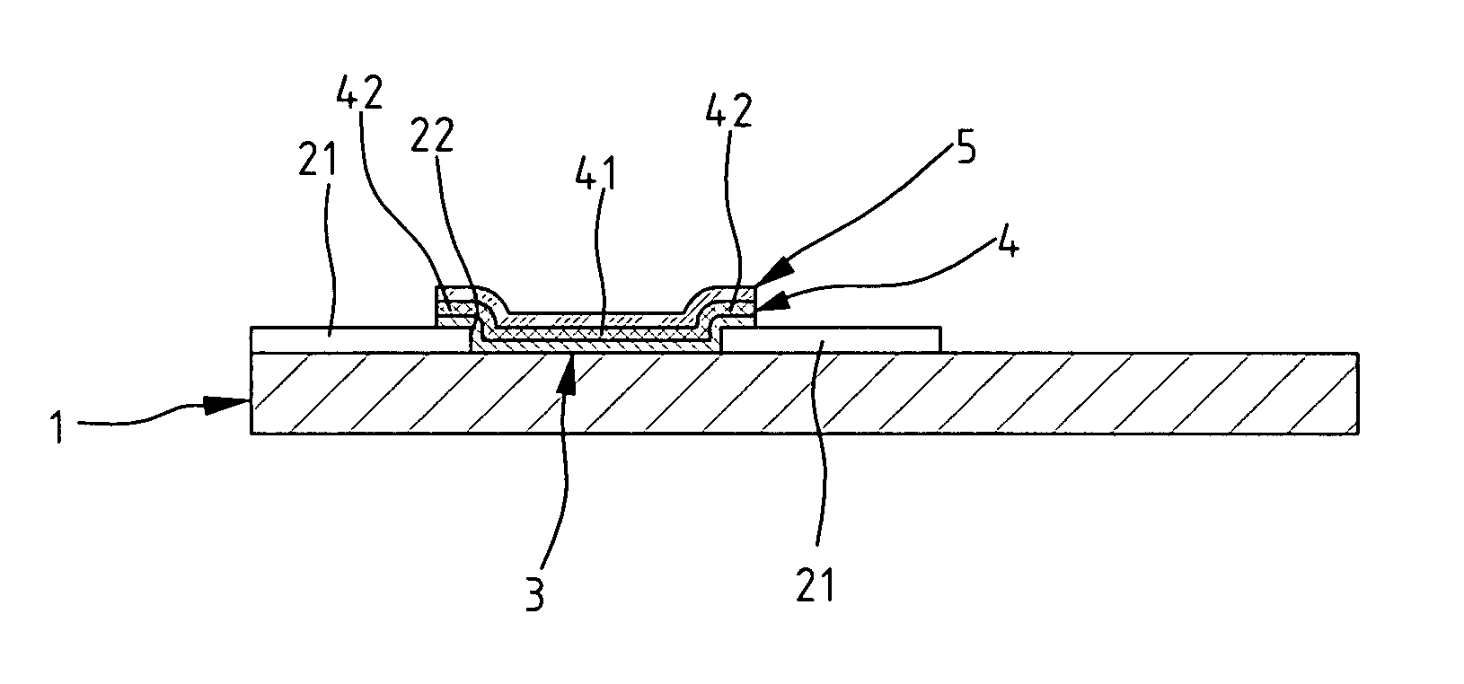
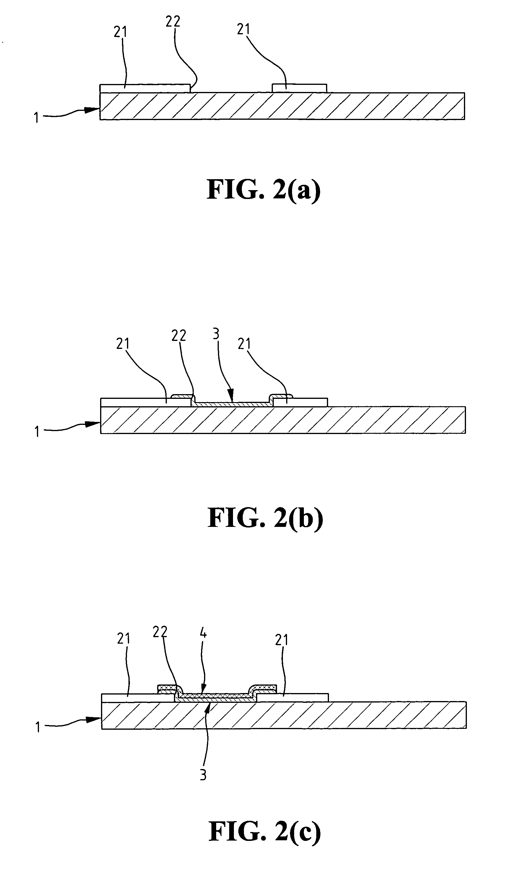
[0015]In step 101, as shown in FIG. 2(a), the conductive wires 21 with resistor wells 22 are formed on a substrate made of an insulating polymer according to layout requirement of circuitry.

[0016]The foregoing conductive wires 21 and resistor wells 22 can be formed using an ordinary printed circuit board fabrication process such as the subtractive, additive, or semi-additive process. The conductive wire 21 is made of copper, aluminum, other well conductive material, or an alloy of the above.

[0017]In step 102, as shown in FIG. 2(b), an activated layer 3 is coated on top of at least surface of each resistor well 22 so as to activate the insulating polymer of the substrate 1 exposed by each resistor well 22.

[0018]The foregoing activated layer 3 is made of activated palladium (Pd) or other ...

second embodiment

[0028]FIG. 3 is a flow chart showing the steps of forming embedded thin film resistors on a printed circuit board according to the present invention. These steps are described sequentially as follows.

[0029]In step 201, as shown in FIG. 4(a), a conductive layer 2 is formed on a substrate 1 made of an insulating polymer. The conductive layer 2 is then processed, based on the locations and dimensions of the resistors required by the printed circuit board, to form the corresponding resistor windows 23.

[0030]The conductive layer 2 is made of copper, aluminum, other well conductive material, or an alloy of the above.

[0031]In step 202, as shown in FIG. 4(b), an activated layer 3 is coated on top of at least surface of each resistor window 23 of the conductive layer 2 so as to activate the insulating polymer of the substrate 1 exposed by each resistor window 23.

[0032]The foregoing activated layer 3 is made of activated palladium (Pd) or other appropriate activator that can be used to form t...


PUM

PropertyMeasurementUnit
conductiveaaaaaaaaaa
insulatingaaaaaaaaaa
volume resistivityaaaaaaaaaa

Abstract

A method for fabricating the embedded thin film resistors of a printed circuit board is provided. The embedded thin film resistors are formed using a resistor layer built in the printed circuit board. Compared with conventional discrete resistors, embedded thin film resistors contribute to a smaller printed circuit board as the space for installing conventional resistors is saved, and better signal transmission speed and quality as the capacitive reactance effect caused by two connectors of the conventional resistors is avoided. The method for fabricating the embedded thin film resistors provided by the invention can be conducted using the process and equipment for conventional printed circuit boards and thereby saving the investment on new types of equipment. The method can be applied in the mass production of printed circuit boards and thereby reduce the manufacturing cost significantly.

Description

CROSS REFERENCE TO RELATED DOCUMENTS[0001]This application claims priority to TAIWAN Application No. 093106057, filed on Mar. 8, 2004.FIELD OF THE INVENTION[0002]The present invention generally relates to a printed circuit board, and more specifically to a method for fabricating embedded thin film resistors of a printed circuit board.BACKGROUND OF THE INVENTION[0003]In general, besides using conventional discrete passive elements, a printed circuit board can also use a thick film or a thin film process to develop the resistors required. In the thick film process, the resistors of the printed circuit board are made of carbon paste printed on the printed circuit board. Then the resistances of the resistors are fine-tuned by the laser trimming. In the thin film process, on the other hand, a nickel-plated copper foil and the epoxy resin of the printed circuit board is pressed together during the fabricating process of the printed circuit board. The nickel-plated side of the copper foil ...

Claims


Application Information

Patent Timeline
Patent Type & Authority Patents(United States)
IPC IPC(8): H01C17/00H01C7/00H01C17/06H01C17/075H01C17/28H05K1/16H05K3/06H05K3/18
CPCH01C7/006H01C17/075H01C17/28H05K1/167H01C17/06Y10T29/49151H05K3/061H05K3/181H05K2203/1453Y10T29/49002Y10T29/4913Y10T29/49082Y10T29/49099Y10T29/49155Y10T29/49098Y10T29/49085Y10T29/53535Y10T29/49126
Inventor SU, SUNG-LINGXU, ZHIQIANG
Owner SU SUNG LING
Why Eureka
Try Eureka