

Silicon single crystal and method for growing silicon single crystal
a single crystal, silicon technology, applied in the direction of polycrystalline material growth, silicon compounds, under protective fluid, etc., can solve the problems of complex process, difficult to ensure the resistivity value of ingots, and complex methods that must be employed for actual implementation of processes, so as to achieve the effect of increasing the segregation coefficient and increasing the yield
Active Publication Date: 2007-05-08
SUMITOMO MITSUBISHI SILICON CORP
View PDF3 Cites 6 Cited by
- Summary
- Abstract
- Description
- Claims
- Application Information
AI Technical Summary
Benefits of technology
"The present invention provides a method for growing a silicon single crystal with a uniform resistivity value and an increased yield. This is achieved by adding a small amount of phosphorus to the initial melt during the Czochralski method, which results in a high apparent segregation coefficient of boron. The technical effect of this method is the ability to produce silicon wafers with the required resistivity value in the longitudinal direction of a p-type rod-like silicon single crystal containing boron as the main additive."
Problems solved by technology
Because the resistivity typically decreases toward the rear part of the single-crystal ingot that has been pulled, when the desired resistivity range is comparatively narrow, there are portions of the ingot with a resistivity outside this desired range and those portions cannot be used as products.
However, this additive should not be melted during initial melting and a complex method has to be employed for actual implementation of the process.
Furthermore, because an additive has to be added to the melt in the course of the crystal growth, certain special tools are required and the process becomes complex.
Therefore, the required resistivity value of the ingot is difficult to ensure, resistivity values of all the wafers have to be measured in the wafer production process, and the process flow often becomes difficult.
Method used
View moreImage
Smart ImageViewing Examples

Examples
embodiment 1
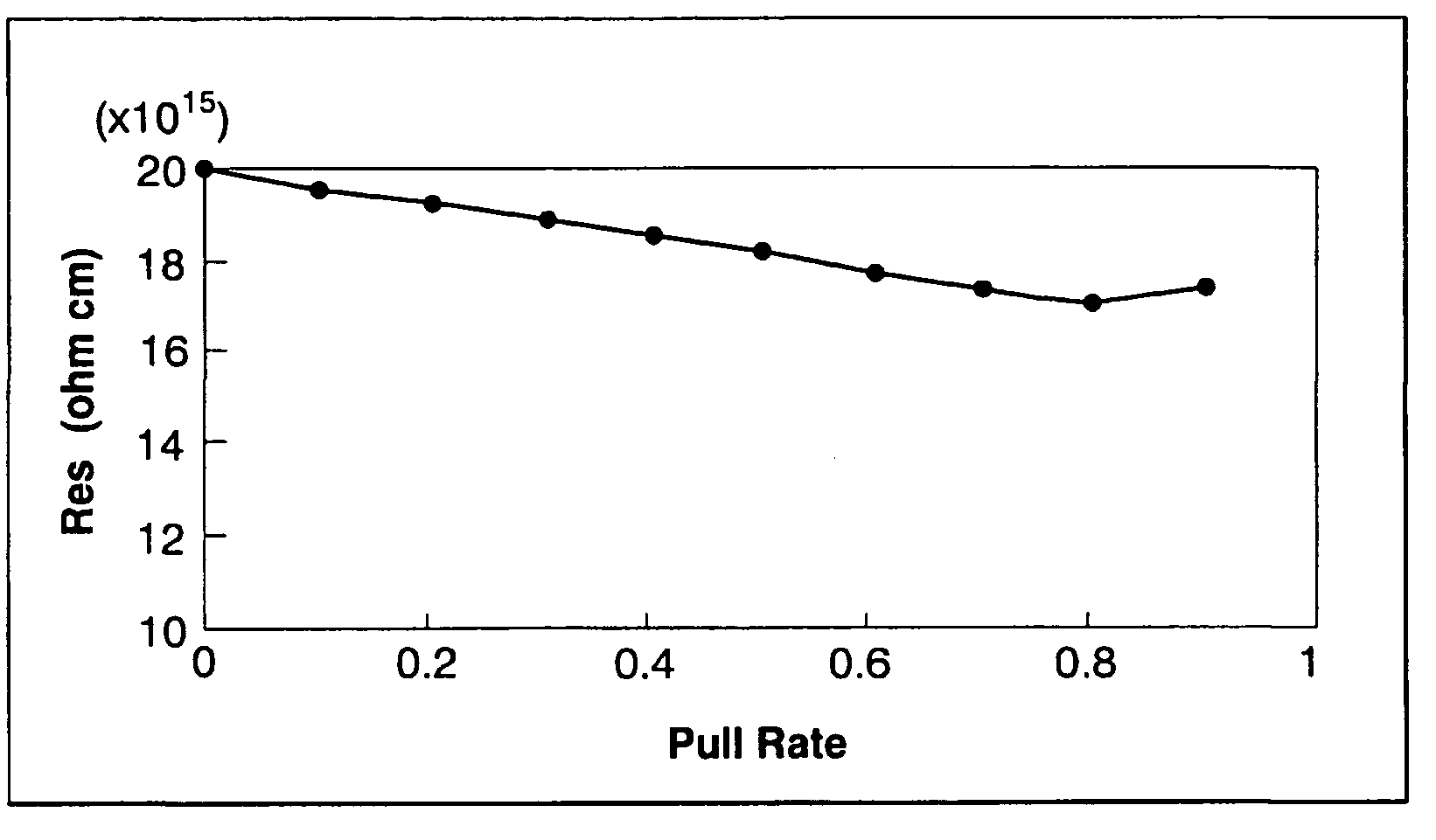
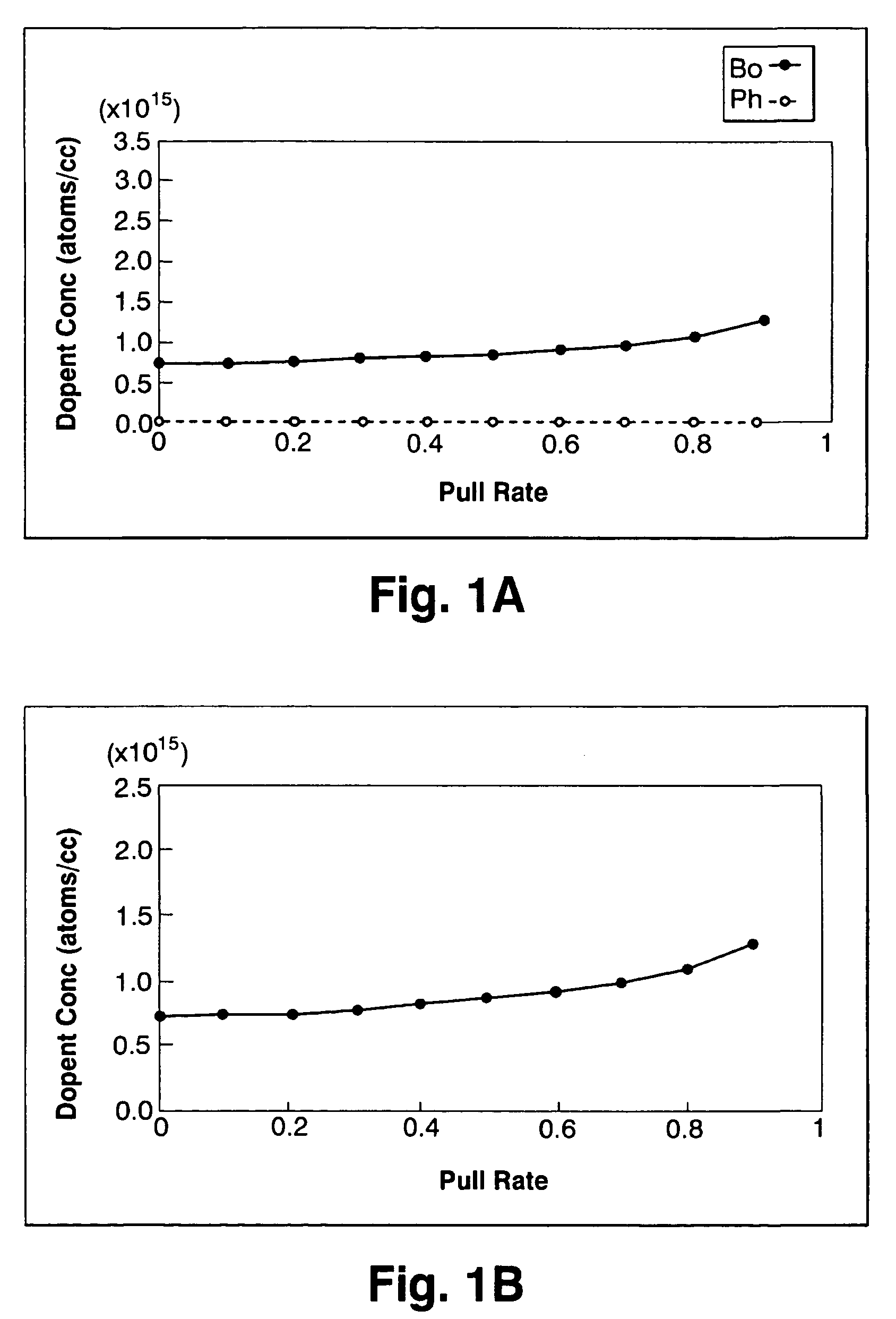
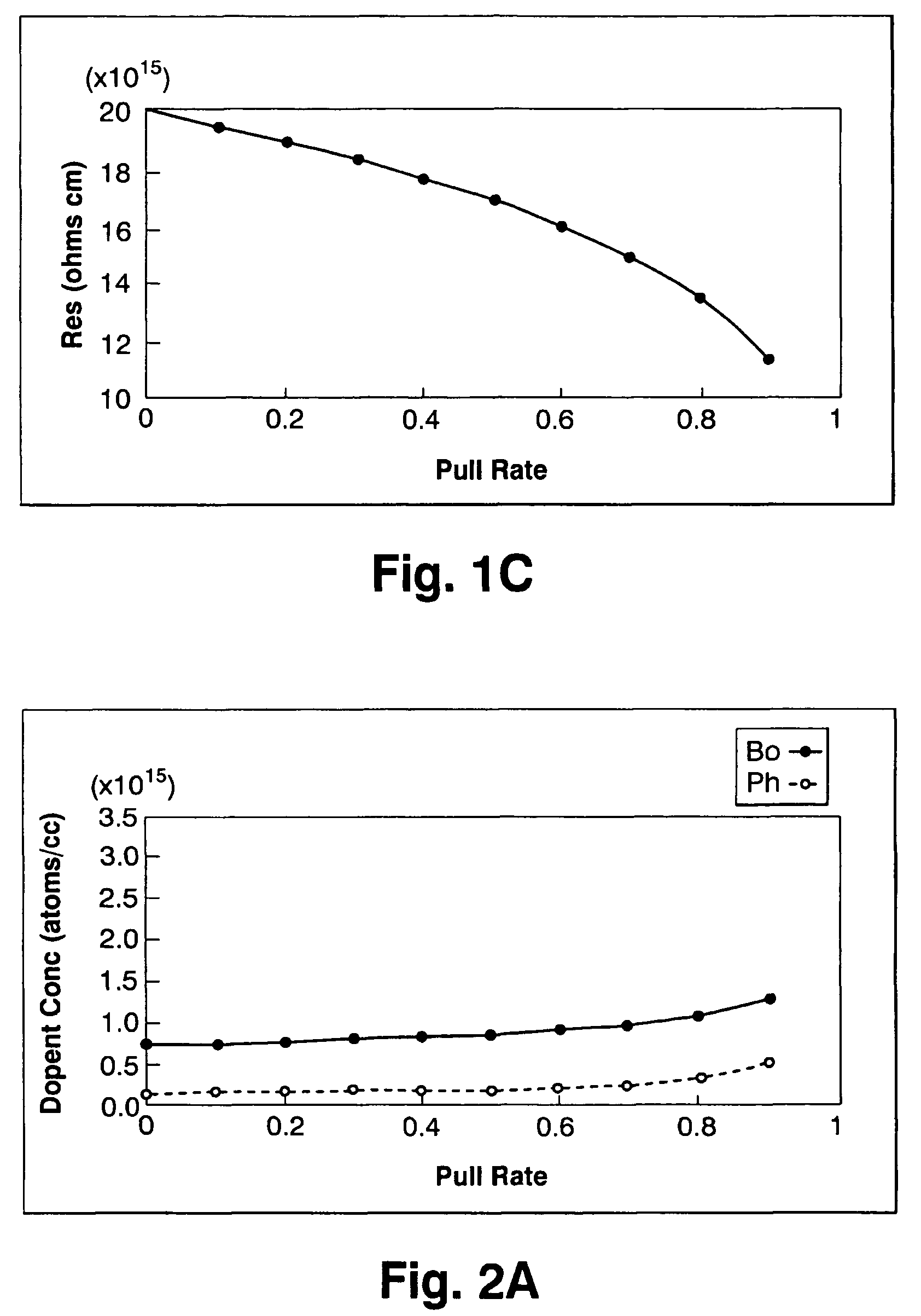
[0026]When melting 140 kg of silicon and growing a p-type 8-inch single crystal with a resistivity of 15˜20 Ωcm in a similar way as in Comparative Example 1, pulling was conducted upon adding phosphorus at 31% of the absolute boron concentration (atoms / cc) in the initial solution.
[0027]As a result, as shown by the concentrations of boron and phosphorus, the difference in the concentration between boron and phosphorus, and the resistivity value in FIG. 2, the desired resistivity value could be obtained in 90% of the entire body. Furthermore, the segregation coefficient of boron in silicon containing no phosphorus was 0.75, but when 31% phosphorus was added, the segregation coefficient became 0.85.
Login to View More PUM
| Property | Measurement | Unit |
|---|---|---|
| resistivity | aaaaa | aaaaa |
| resistivity | aaaaa | aaaaa |
| concentration | aaaaa | aaaaa |
Abstract
A silicon single crystal and a method for growing a silicon single crystal are provided. A p-type silicon single crystal is grown with a uniform resistivity value in a pulling direction. Pulling is conducted by the Czochralski method from molten silicon obtained by adding phosphorus to an initial melt in an amount equivalent to 25˜35% of an absolute concentration (atoms / cc) of boron contained in the melt.
Description
BACKGROUND OF THE INVENTION[0001]1. Field of the Invention[0002]The present invention relates to a method for growing a p-type silicon single crystal for silicon wafers used as semiconductor materials, more particularly to a method for growing a silicon single crystal with excellent yield which makes it possible to obtain a larger number of silicon wafers with a required resistivity value in the longitudinal direction of a rod-like single crystal.[0003]2. Description of the Prior Art[0004]When a silicon single crystal having a desired resistivity is grown by the Czochralski method, a segregation coefficient inherent to the substance and determined by the type of silicon and additives has to be taken into account. Because the resistivity typically decreases toward the rear part of the single-crystal ingot that has been pulled, when the desired resistivity range is comparatively narrow, there are portions of the ingot with a resistivity outside this desired range and those portions ca...
Claims
Login to View More Application Information
Patent Timeline
 Patent Type & AuthorityPatents(United States)
IPC IPC(8): C30B15/04C30B15/00C30B29/06
CPCC30B15/04C30B29/06
InventorKATO
OwnerSUMITOMO MITSUBISHI SILICON CORP