Method of producing P-doped silicon single crystal and P-doped N-type silicon single crystal wafer

a technology of n-type silicon and single crystal, which is applied in the direction of crystal growth process polycrystalline material growth, etc., can solve the problems of low yield, and difficult control of single crystal productivity, etc., to achieve high breakdown voltage, easy and inexpensive production, excellent electrical characteristics

Active Publication Date: 2007-05-08
SHIN-ETSU HANDOTAI CO LTD
View PDF4 Cites 4 Cited by
  • Summary
  • Abstract
  • Description
  • Claims
  • Application Information

AI Technical Summary

Benefits of technology

[0014]Accordingly, the present invention was conceived in view of the above problems. An object of the present invention is to provide a method of easily and inexpensively producing a P-doped silicon single crystal of defect-free region having an excellent capability of electrical characteristics to be high breakdown voltage, which contains neither, for example, V region, OSF region, nor large dislocation cluster (LSEPD, LFPD) region, and to provide the P-doped N-type silicon single crystal wafer.

Problems solved by technology

It is difficult to control the rate because the single crystal of N region can be grown in a range of a relatively limited pulling rate.
Thus, productivity and yield of the single crystal become low.

Method used


Image

  • Method of producing P-doped silicon single crystal and P-doped N-type silicon single crystal wafer
  • Method of producing P-doped silicon single crystal and P-doped N-type silicon single crystal wafer
  • Method of producing P-doped silicon single crystal and P-doped N-type silicon single crystal wafer

Examples


example 1

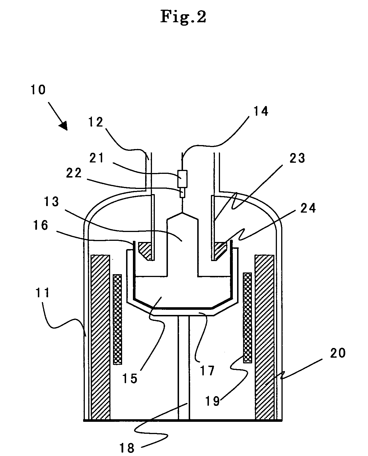
[0047]A silicon single crystal was produced by using a single crystal production apparatus as shown in FIG. 2. 150 kg of raw material polycrystal silicon and 4 mg of refined Al metal grains were charged in the quartz crucible with a diameter of 24 inches (600 mm), and a silicon single crystal with a diameter of 210 mm and orientation was pulled. When pulling the silicon single crystal, a growth rate was controlled so as to be gradually decreased from a head of the crystal through a tail thereof in a range from 0.60 mm / min to 0.20 mm / min. Moreover, the silicon single crystal was produced so that a P concentration might be 3×10¹⁴ to 5.5×10¹⁴ atoms / cc and oxygen concentration might be 24–27 ppma (ASTM'79).

[0048]A straight body of each silicon single crystal ingot grown as described above was cut into blocks by each length of 10 cm along a crystal growth axis as shown in FIG. 3(a), and thereafter each block was cut longitudinally along the crystal axis and several samples with thicknes...

example 2

[0056]A silicon single crystal was produced and each measurement was performed as the same with Example 1 except for charging 150 kg of raw material polycrystal silicon and 8 mg of refined Al metal grains in a quartz crucible.

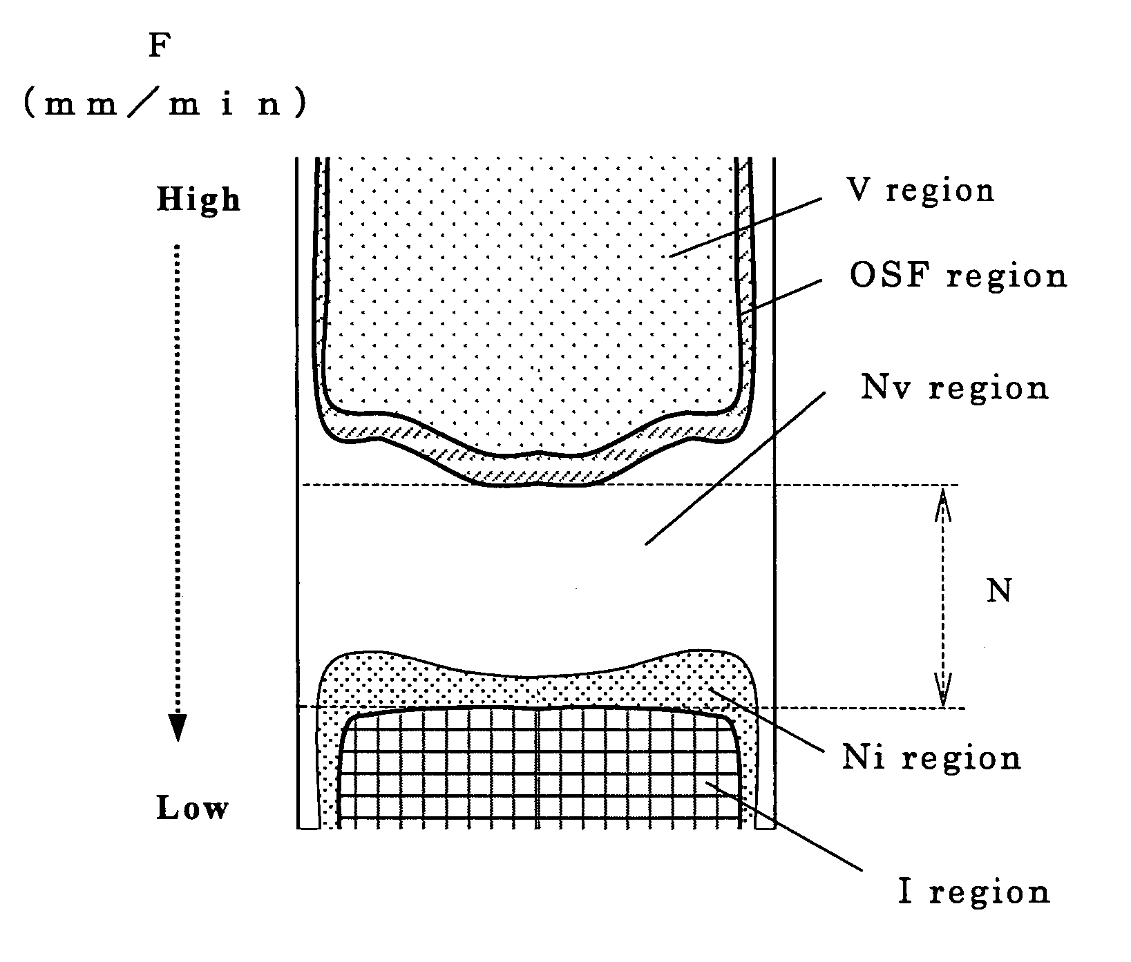
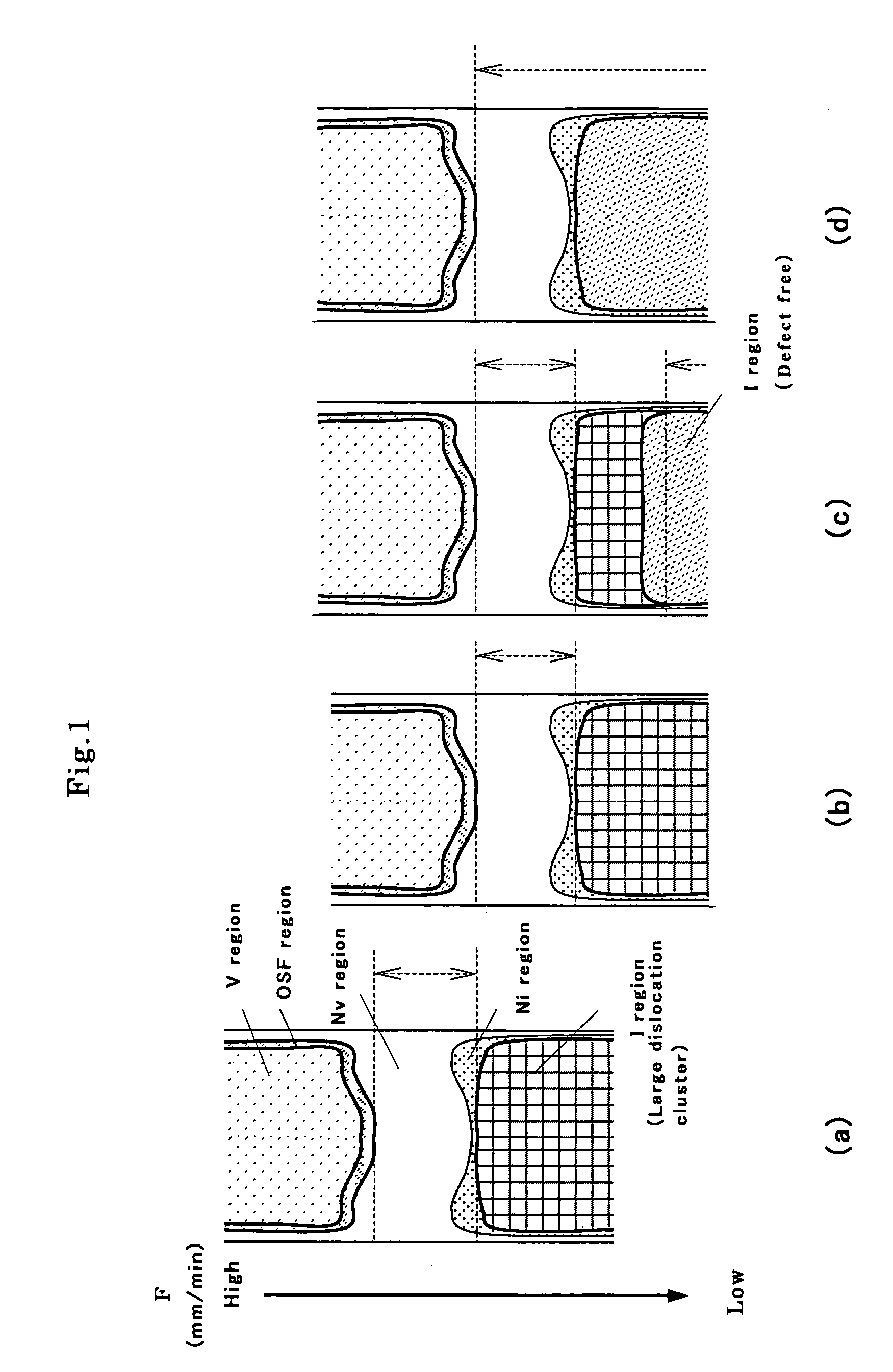
[0057]More detailed distribution of each region which was found from the above-described measurement is shown in FIG. 1(d). F / G (mm2 / ° C.·min) and an Al concentration in each region boundary are shown as follows.

[0058]F / G (mm2 / ° C.·min) in the boundary between OSF region and N region: 0.20

[0059]F / G (mm2 / ° C.·min) in the boundary between N region and (defect-free) I region: 0.18 an Al concentration in the crystal bulk near

[0060]F / G=0.17:8.8×10¹² atoms / cc.


PUM

PropertyMeasurementUnit
melting pointaaaaaaaaaa
diameteraaaaaaaaaa
sizeaaaaaaaaaa

Abstract

The present invention is a method of producing a P(phosphorus)-doped silicon single crystal by Czochralski method, wherein, at least, a growth of the single crystal is performed so that an Al (aluminum) concentration is 2×10¹² atoms / cc or more. Thereby, there can be provided a method of easily and inexpensively producing a P(phosphorus)-doped silicon single crystal of defect-free region having an excellent capability of electrical characteristics to be high breakdown voltage, which contains neither, for example, V region, OSF region, nor large dislocation cluster (LSEPD, LFPD) region.

Description

TECHNICAL FIELD[0001]The present invention relates to a method of producing a P-doped silicon single crystal by Czochralski method and a P-doped N-type silicon single crystal wafer. Particularly, the present invention relates to a method of producing a P-doped silicon single crystal of defect-free region having an excellent capability of electrical characteristics to be high breakdown voltage, which contains neither V region, OSF region, nor large dislocation cluster (LSEPD, LFPD) region, and to a P-doped N-type silicon single crystal wafer.BACKGROUND ART[0002]A single crystal used as a substrate of semiconductor devices, for example, a silicon single crystal, is mainly produced by Czochralski method (hereafter abbreviated to CZ method).[0003]When producing a single crystal by CZ method, for example, a single crystal production apparatus 10 as shown FIG. 2 is used to produce the single crystal. This single crystal production apparatus 10 has a member for containing and melting a raw...

Claims


Application Information

Patent Timeline
Patent Type & Authority Patents(United States)
IPC IPC(8): C30B15/20C30B15/00C30B29/06C30B15/04
CPCC30B15/04C30B15/203C30B29/06H01L21/20
Inventor SAKURADA, MASAHIROFUSEGAWA, IZUMI
Owner SHIN-ETSU HANDOTAI CO LTD
Why Eureka
Try Eureka