Device for amplitude adjustment and rectification made with MOS technology

a technology of amplitude adjustment and rectification, applied in the direction of negative-feedback-circuit arrangement, ac-dc conversion, gain control, etc., can solve the problems of amplitude compression device problems, amplitude compression device manufacturing in accordance with the mos process, and the driver is difficult to listen to the piano sounds which are performed in pianissimo

Inactive Publication Date: 2007-05-08
YAMAHA CORP
View PDF14 Cites 4 Cited by
  • Summary
  • Abstract
  • Description
  • Claims
  • Application Information

AI Technical Summary

Benefits of technology

[0019]It is an object of the invention to provide an amplitude compression device and an amplitude expansion device, which have simple circuit configurations and which can be manufactured as ICs in accordance with the MOS process with ease.
[0023]In another aspect of the invention, there is provided a full-wave rectifier, applicable to the amplitude adjustment device, which is mainly configured by an inversion amplifier, an amplifier and an output section. Herein, the inversion amplifier amplifies an input signal with a gain of “−1”, while the amplifier amplifies it with a gain of “1”. Outputs of the amplifiers differ from each other in phases by 180°. The output section produces a full-wave rectified signal based on the outputs of the amplifiers. Specifically, the output section selects either the output signal of the inversion amplifier or the output signal of the amplifier in response to every half of one period of the input signal. For example, the output signal of the inversion amplifier is selected and is used for formation of a first portion of a full-wave rectified signal in a first half duration of one period of the input signal. In addition, the output signal of the amplifier is selected and is used for formation of a second portion of the full-wave rectified signal in a second half duration. The first and second portions are combined together to form a “negative” waveform for the full-wave rectified signal in response to one period of the input signal. Incidentally, all of the amplifiers and output section are configured using field-effect transistors without using diodes being externally connected. Hence, it is possible to manufacture the full-wave rectifier in a form of an IC in accordance with the MOS process with ease.

Problems solved by technology

So, if the drivers play back the music having a broad dynamic range such as the classic music, the drivers are hard to listen to piano sounds which are performed in pianissimo, for example.
The aforementioned examples of the amplitude compression devices suffer from problems, as follows:
So, it is impossible to manufacture the amplitude compression device in a form of an IC in accordance with the MOS process (or MOS technology).
For this reason, the first example of the amplitude compression device suffers from a problem in which it has a limited range of application.
Thus, the second example suffers from a problem in which it cannot produce the output signal which is “smooth”.
For this reason, the third example suffers from a problem in which it has a complicated circuit configuration.
However, it is impossible to form the diodes by the CMOS process.
So, there is a disadvantage in that the diodes should be provided as external components which are attached to the LSI circuit.

Method used


Image

  • Device for amplitude adjustment and rectification made with MOS technology
  • Device for amplitude adjustment and rectification made with MOS technology
  • Device for amplitude adjustment and rectification made with MOS technology

Examples


embodiment 1

[A] Embodiment 1

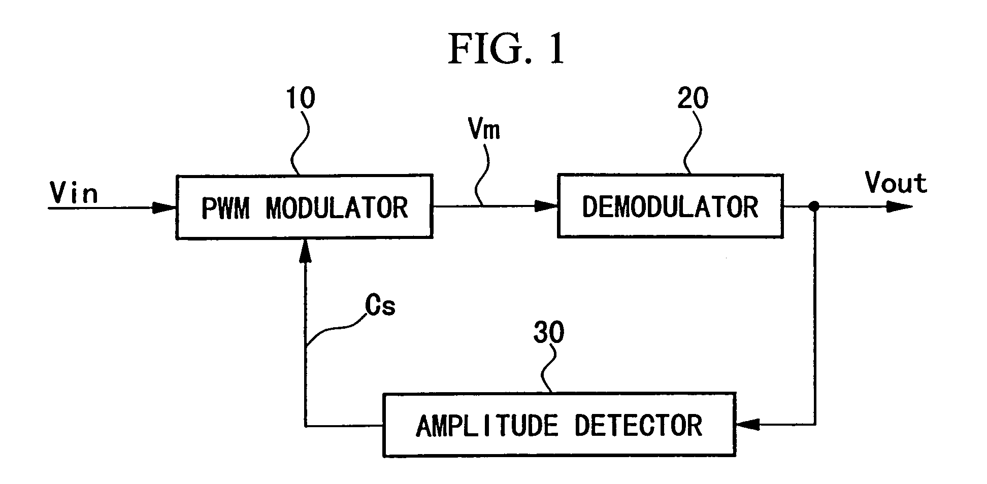
[0052]Now, a description will be given with respect to a circuit configuration of an amplitude compression device in accordance with embodiment 1 of the invention. FIG. 1 is a block diagram showing the amplitude compression device of the embodiment 1. The amplitude compression device of FIG. 1 contains a PWM modulator 10 (where “PWM” is an abbreviation for “Pulse-Width Modulation”), a main part of which is configured by a self-sustaining oscillation circuit. Herein, the PWM modulator 10 performs pulse-width modulation on an input signal Vin in response to a modulation factor, which is determined by a control signal Cs. Thus, the PWM modulator 10 produces and outputs a pulse-width modulated signal Vm.

[0053]A demodulator 20 is configured using a low-pass filter. The demodulator 20 demodulates the pulse-width modulated signal Vm to produce an output signal Vout. The low-pass filter has “flat” frequency characteristics in a frequency band of the input signal Vin. In addi...

embodiment 2

[B] Embodiment 2

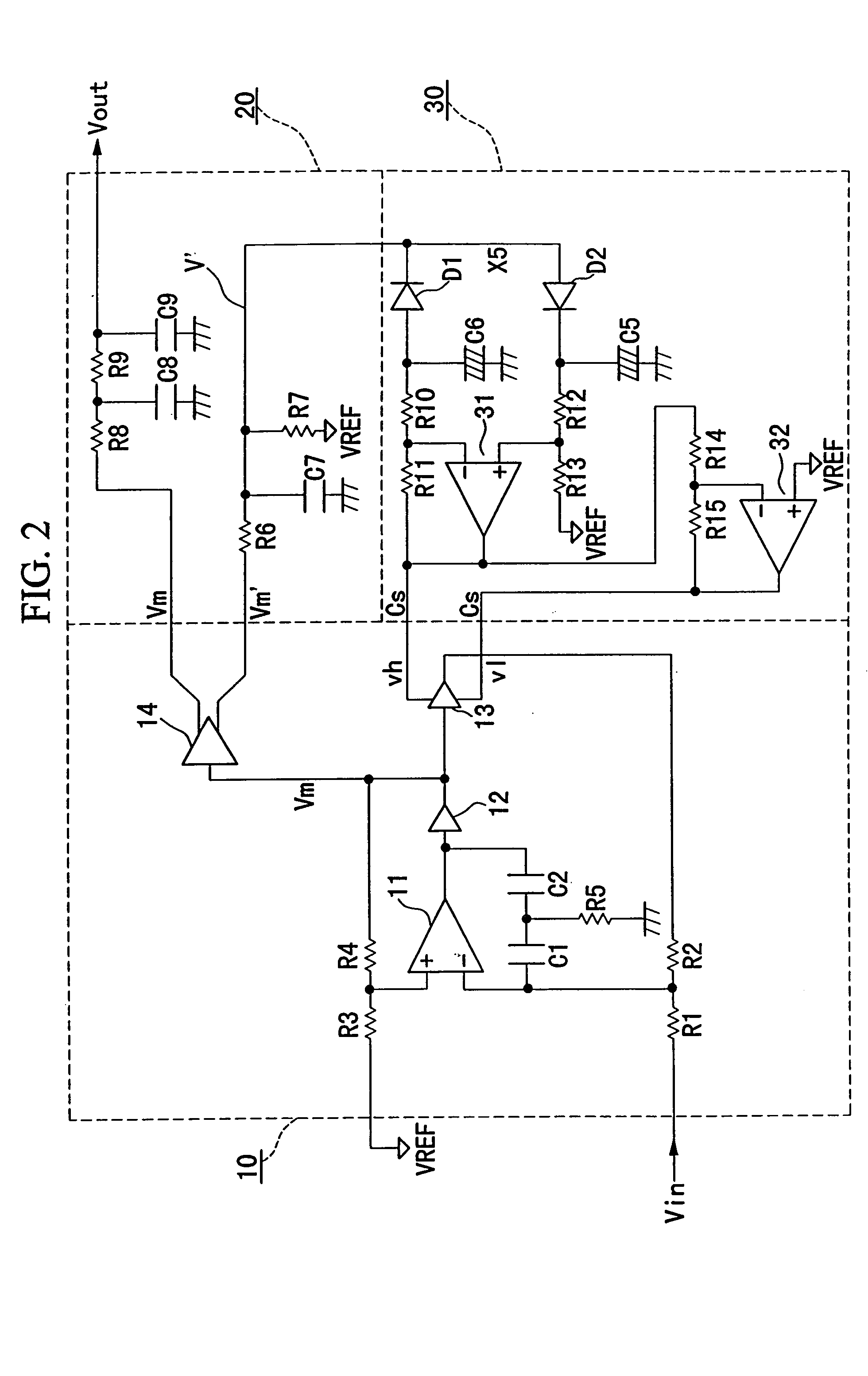
[0077]Next, a description will be given with respect to a configuration of an amplitude compression device in accordance with embodiment 2 of the invention.

[0078]FIG. 5 is a block diagram showing the amplitude compression device of the embodiment 2. Like the aforementioned embodiment 1 shown in FIG. 1, the amplitude compression device of the embodiment 2 is configured by the PWM modulator 10, the demodulator 20 and the amplitude detector 30. However, different from the embodiment 1 in which the output signal Vout is detected to produce the control signal Cs, the embodiment 2 is designed such that the amplitude detector 30 detects the amplitude of the input signal Vm to produce the control signal Cs. In other words, the embodiment 1 is configured in a feedback form, while the embodiment 2 is configured in a feed-forward form.

[0079]FIG. 6 is a circuit diagram showing internal circuit configurations of the amplitude compression device of the embodiment 2, wherein parts ...

embodiment 4

[D] Embodiment 4

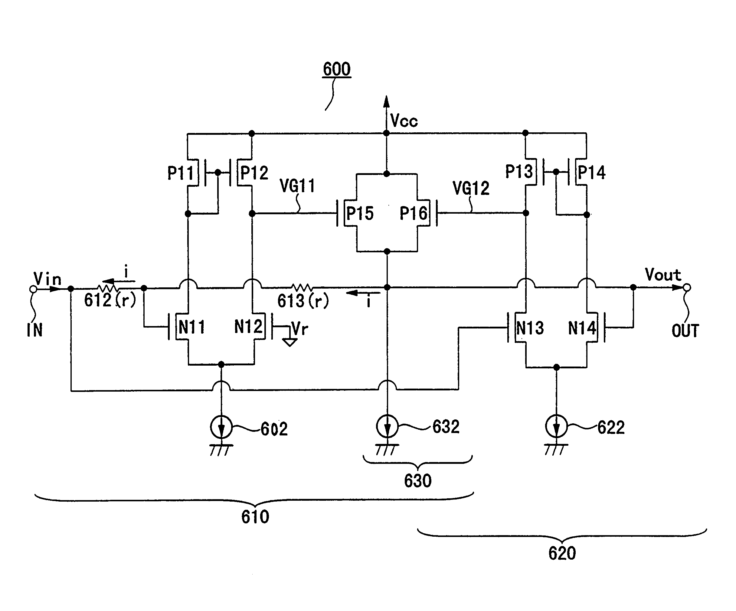
[0105]The aforementioned full-wave rectifier 500 of the embodiment 3 is designed to produce the “negative” output signal Vout. In contrast, a full-wave rectifier 600 of the embodiment 4 is designed to produce a “positive” output signal Vout.

[0106]FIG. 9 is a circuit diagram showing circuit configurations of the full-wave rectifier 600 in accordance with the embodiment 4, wherein parts equivalent to those of FIG. 7 are designated by the same reference symbols.

[0107]The full-wave rectifier 600 of FIG. 9 is mainly configured by an inversion amplifier 610, an amplifier 620 and an output section 630, which are basically equivalent to the inversion amplifier 510, the amplifier 520 and the output section 530 shown in FIG. 7.

[0108]The inversion amplifier 610 is configured by a constant current source 602, a pair of n-channel FETs N11, N12, a pair of p-channel FETs P11, P12 which act as active loads, and resistors 612, 613 as well as the output section 630. In the inversion a...


PUM


Abstract

An amplitude adjustment device such as an amplitude compression device and amplitude expansion device is basically configured by a PWM modulator, a demodulator and an amplitude detector. Herein, the PWM modulator effects pulse-width modulation on an input signal to produce a pulse-width modulated signal, which is demodulated by the demodulator to produce an output signal. In addition, the amplitude detector detects an amplitude of a demodulated signal or an amplitude of the input signal to produce a control signal. A modulation factor of the pulse-width modulation is adjusted based on the control signal. In the case of the amplitude compression device, an input / output gain is changed inversely proportional to the amplitude of the input signal or amplitude of the output signal. Thus, it is possible to compress a dynamic range with respect to input / output characteristics. A full-wave rectifier, applicable to the amplitude adjustment device, is mainly configured by an inversion amplifier, an amplifier and an output section. Herein, the inversion amplifier amplifies an input signal with a gain of “−1”, while the amplifier amplifies it with a gain of “1”. Outputs of the amplifiers differ from each other in phases by 180°. The output section produces a full-wave rectified signal based on the outputs of the amplifiers. Incidentally, all of the amplifiers and output section are configured using field-effect transistors without using diodes being externally connected. Hence, it is possible to manufacture the full-wave rectifier in a form of an IC in accordance with the MOS process with ease.

Description

BACKGROUND OF THE INVENTION[0001]1. Field of the Invention[0002]This invention relates to amplitude adjustment devices such as amplitude compression devices and amplitude expansion devices, which are made with the MOS (i.e., Metal-Oxide Semiconductor) technology. In addition, this invention also relates to full-wave rectifiers, applicable to the amplitude adjustment devices, which are made with the MOS technology. Specifically, the devices are used for amplitude adjustment and rectification of audio inputs of digital audio systems.[0003]This application is based on Patent Application No. Hei 10-180864 and Patent Application No. Hei 10-180865 both filed in Japan, the contents of which are incorporated herein by reference.[0004]2. Description of the Related Art[0005]Conventionally, amplitude compression / expansion devices are used for compressing and expanding signals of audio playback systems or audio reproduction systems. In the case of the automobiles, for example, drivers normally ...

Claims


Application Information

Patent Timeline
Patent Type & Authority Patents(United States)
IPC IPC(8): H03F3/38H03F3/52H03G3/30H03K7/08
CPCH03G3/3026H03K7/08
Inventor MAEJIMA, TOSHIO
Owner YAMAHA CORP
Why Eureka
Try Eureka