Substrate for electronic device, electronic device and methods of manufacturing same

a technology of electronic devices and substrates, applied in the direction of solid-state devices, semiconductor devices, mechanical vibration separation, etc., can solve the problems of affecting the reliability of the process and the electronic device, the inability to form epitaxial films on such a base layer, and the inability to fabricate excellent crystallinity conductor films, so as to achieve the effect of improving the crystallinity the adhesion of the conductor films to the bas

Active Publication Date: 2007-05-22
SNAPTRACK
View PDF6 Cites 8 Cited by
  • Summary
  • Abstract
  • Description
  • Claims
  • Application Information

AI Technical Summary

Benefits of technology

[0019]According to the substrate for the electronic device or the method of manufacturing the same of the invention, the adhesion film is disposed between the base and the conductor film, the adhesion film being made of a non-epitaxial film including a crystal having a wurtzite crystal structure. As a result, the crystallinity of the conductor film and the adhesion of the conductor film to the base are both improved.

Problems solved by technology

As a result, there arises a problem that it is difficult to fabricate the conductor film having an excellent crystallinity because, for example, a process performed at a temperature of 900° C. or higher is required.
When an epitaxial film is intended to be formed directly on the substrate, the following problem may arise.
Therefore, if the base layer is made of an amorphous material such as glass or silicon oxide, it is impossible to form an epitaxial film on such a base layer.
It is possible to easily obtain a Pt thin film having an excellent crystallinity in which the (111) plane is single-oriented to be parallel to the substrate surface through a method in which a film of silicon oxide or silicon nitride, for example, is formed on a silicon (Si) substrate, and on this film, a platinum (Pt) thin film as a conductor film is vacuum-deposited at a temperature around 500° C. However, the Pt thin film has a serious problem that an absolute contact is not established between the Pt thin film and the base layer and the Pt thin film is easily removed, which affects the reliability of the process and the electronic device.
If a Pt film is formed directly on a glass substrate, the contact between the glass substrate and the Pt film is not sufficient.
If a metal thin film is formed directly on a Si substrate, silicide is likely to be formed and it is difficult to obtain a metal thin film having a good crystallinity.
Through this method, however, it is impossible to form a metal thin film having a crystallinity sufficient for forming a functional film having a good crystallinity on the metal thin film.

Method used


Image

  • Substrate for electronic device, electronic device and methods of manufacturing same
  • Substrate for electronic device, electronic device and methods of manufacturing same
  • Substrate for electronic device, electronic device and methods of manufacturing same

Examples


first example

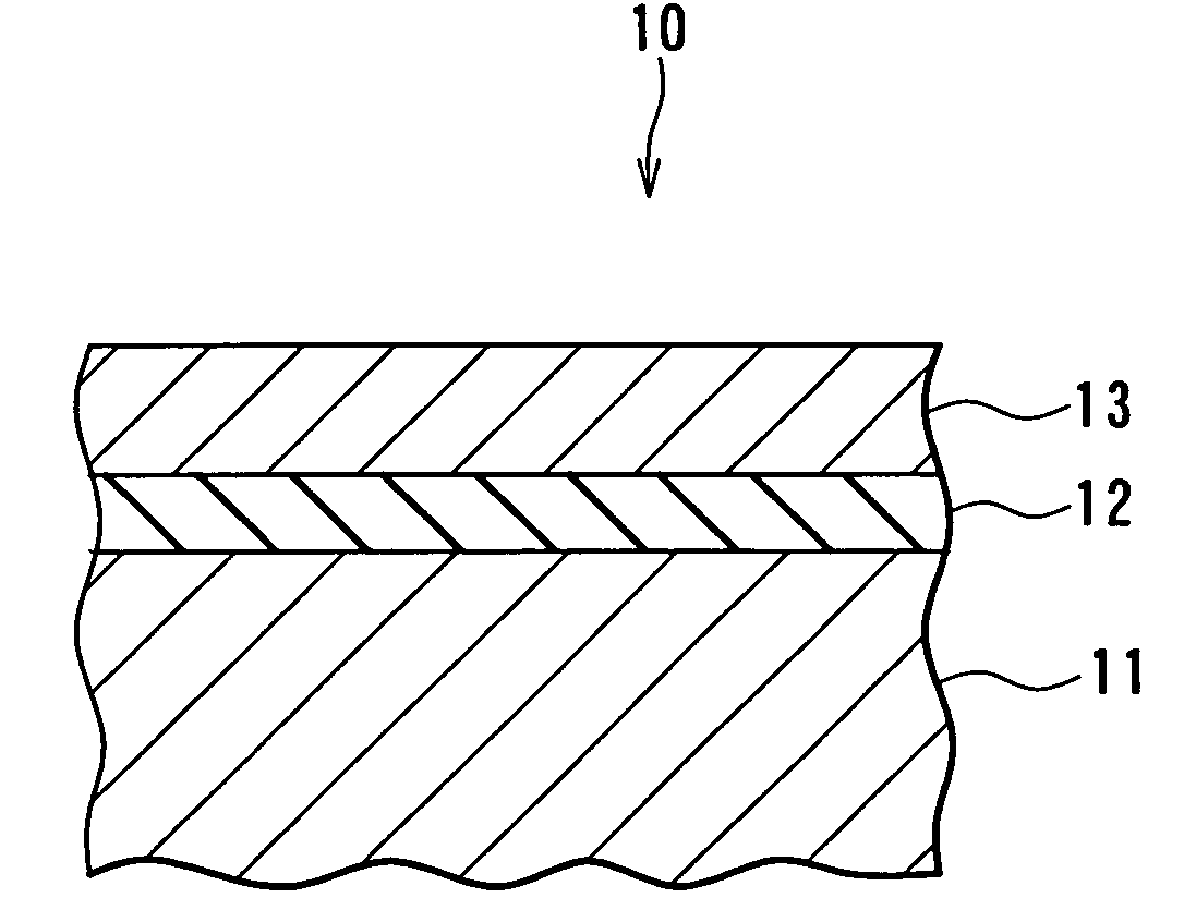
[0088]A first example is an example of the substrate 10 for the electronic device. The base 11 of the substrate 10 of this example was made of a substrate of single-crystal Si having a surface on which a thermal-oxidized SiO2 film was formed. The substrate had a thickness of 250 μm and a resistivity of 1000 ohm-cm. The (100) plane of the single-crystal Si was parallel to the surface of the substrate. The surface of the substrate had been mirror-ground in advance and the thermal-oxidized SiO2 film was formed on this surface.

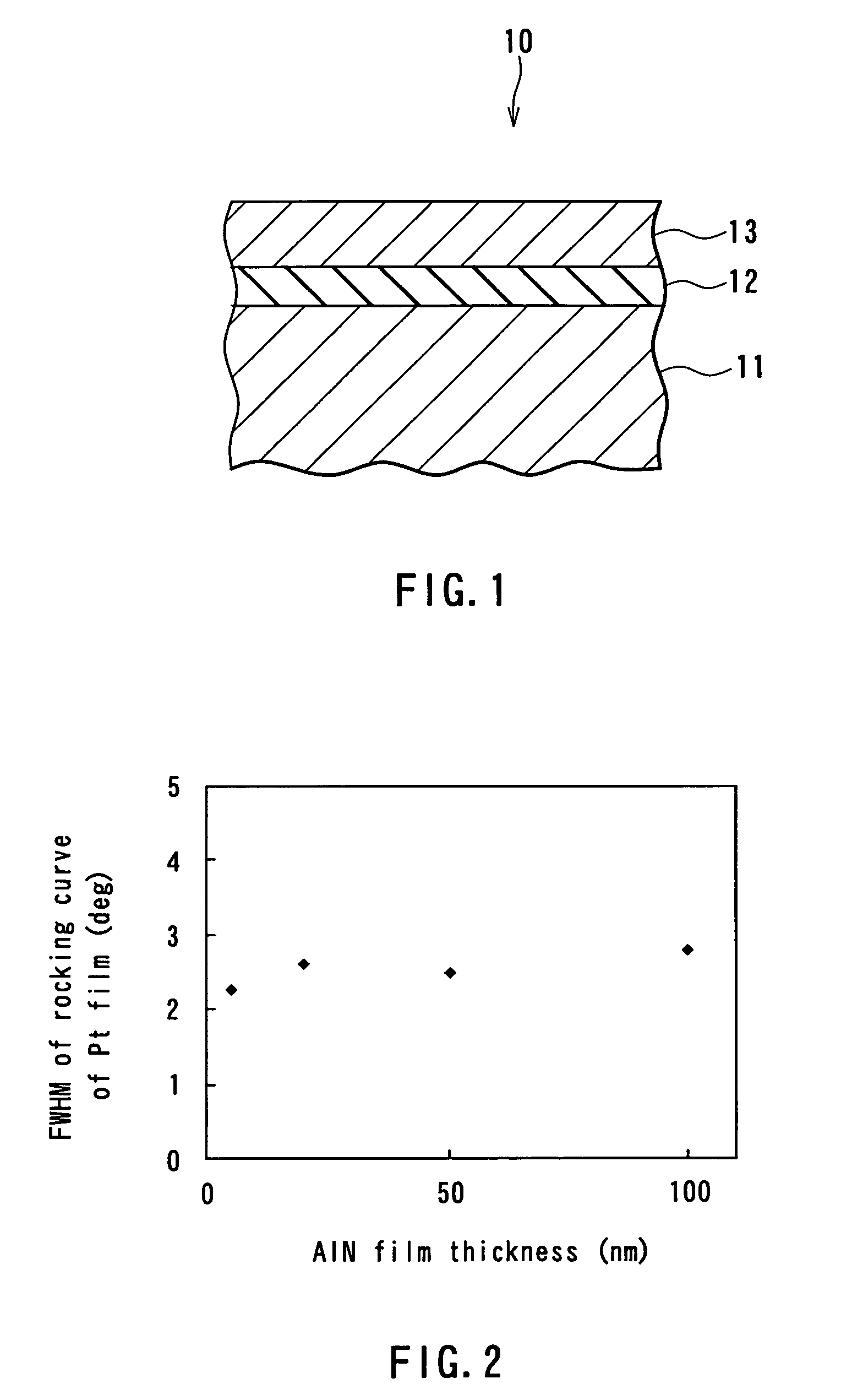
[0089]According to the substrate 10 of the example, an AlN film having a thickness of 50 nm as the adhesion film 12 was formed on the base 11. The AlN film was formed as follows. The base 11 was introduced to a vacuum chamber and the chamber was exhausted so that the pressure therein was 1×10⁻⁴ Pa. Next, a mixed gas of Ar and N2 at a flow rate of 25 sccm was introduced to the chamber so that the pressure therein was 0.4 Pa while the temperature of the base 11 was ...

second example

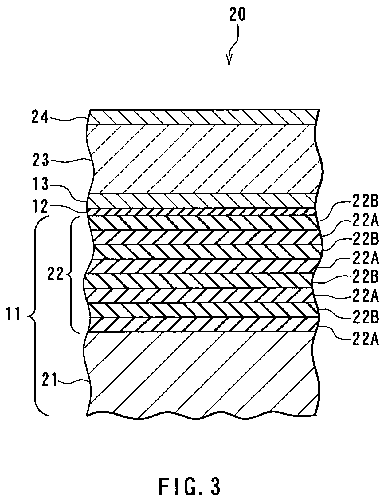
[0095]A second example is an example of the substrate 10 for the electronic device, too. The base 11 of the substrate 10 of this example was made of a substrate of single-crystal Si on which an acoustic reflection film was formed. The substrate had a thickness of 250 μm and a resistivity of 1000 ohm-cm. The (100) plane of the single-crystal Si was parallel to the surface of the substrate. The surface of the substrate had been mirror-ground in advance. The acoustic reflection film was formed by stacking four Al2O3 films each having a thickness of 1500 nm as the first dielectric layers 22A and four SiO2 films each having a thickness of 800 nm as the second dielectric layers 22B alternately in this order on the cleaned surface of the substrate. The Al2O3 films and the SiO2 films were formed by sputtering.

[0096]According to the substrate 10 of the example, on the base 11, an AlN film having a thickness of 50 nm was formed as the adhesion film 12. The AlN film was formed by reactive RF m...

third example

[0100]A third example is an example of the electronic device 20. The base 11 of the electronic device 20 of this example was made of a substrate of single-crystal Si on which an acoustic reflection film was formed. The substrate had a thickness of 250 μm and a resistivity of 1000 ohm-cm. The (100) plane of the single-crystal Si was parallel to the surface of the substrate. The surface of the substrate had been mirror-ground in advance. The acoustic reflection film was formed by stacking four AlN films each having a thickness of 1500 nm as the first dielectric layers 22A and four SiO2 films each having a thickness of 800 nm as the second dielectric layers 22B alternately in this order on the cleaned surface of the substrate. The AlN films were formed by sputtering while the SiO2 films were formed by CVD.

[0101]According to the electronic device 20 of the example, on the base 11, an AlN film having a thickness of 50 nm was formed as the adhesion film 12. The AlN film was formed by a me...


PUM


Abstract

A substrate for an electronic device comprises a base, an adhesion film stacked on the base, and a conductor film stacked on the adhesion film. The adhesion film is a non-epitaxial film including a crystal having a wurtzite crystal structure. The electronic device comprises the substrate and a functional film having a specific function and disposed on the substrate.

Description

BACKGROUND OF THE INVENTION[0001]1. Field of the Invention[0002]The present invention relates to a substrate for an electronic device, an electronic device, and methods of manufacturing such a substrate and an electronic device that are applied to semiconductor devices such as light-emitting diodes and laser diodes, dielectric devices such as thin-film capacitors and ferroelectric nonvolatile memories, and piezoelectric devices such as thin-film bulk acoustic oscillators and surface acoustic wave elements.[0003]2. Description of the Related Art[0004]A variety of electronic devices have been designed and made practical. Such electronic devices are made of various types of substrates on which functional films made of, for example, semiconductors, dielectrics or piezoelectric materials are formed. Examples of electronic devices using semiconductor films are light-emitting diodes and semiconductor lasers. Examples of electronic devices using dielectric films are ferroelectric nonvolatil...

Claims


Application Information

Patent Timeline
Patent Type & Authority Patents(United States)
IPC IPC(8): H01L27/15H01L21/28B06B1/06H01L21/283H01L21/8246H01L27/105H01L41/09H01L41/187H01L41/22H01L41/29H01L41/319H03H3/02H03H9/02H03H9/17
CPCB06B1/0644H03H3/02H03H9/02094H03H9/175H03H9/176H01L41/319H10N30/079
Inventor NOGUCHI, TAKAOSAITOU, HISATOSHIABE, HIDENORI
Owner SNAPTRACK
Why Eureka
Try Eureka