Method of fabricating a ceramic substrate with a thermal conductive plug of a multi-chip package

a technology of ceramic substrate and thermal conductive plug, which is applied in the direction of printed circuit aspects, conductive pattern formation, printed element electric connection formation, etc., can solve the problems of high energy consumption, high heat dissipation problem, and high cost, so as to reduce production cost

Active Publication Date: 2007-05-29
NAT CHUNG SHAN INST SCI & TECH
View PDF6 Cites 22 Cited by
  • Summary
  • Abstract
  • Description
  • Claims
  • Application Information

AI Technical Summary

Benefits of technology

[0008]It is an object of the present invention provides a method of fabricating a ceramic substrate with a thermal conductive plug of

Problems solved by technology

Due to the complicated functions of the chip, a lot of heat dissipating problems are still required to be resolved.
However, since the hardness of the ceramic substrate is very high, and the ceramic substrate is very brittle plus its measurement is very thick.
However, in order to penetrate through the high hardness of thick ceramic substrate, a lot of ene

Method used


Image

  • Method of fabricating a ceramic substrate with a thermal conductive plug of a multi-chip package
  • Method of fabricating a ceramic substrate with a thermal conductive plug of a multi-chip package
  • Method of fabricating a ceramic substrate with a thermal conductive plug of a multi-chip package

Examples


Embodiment Construction

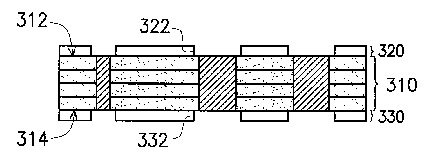
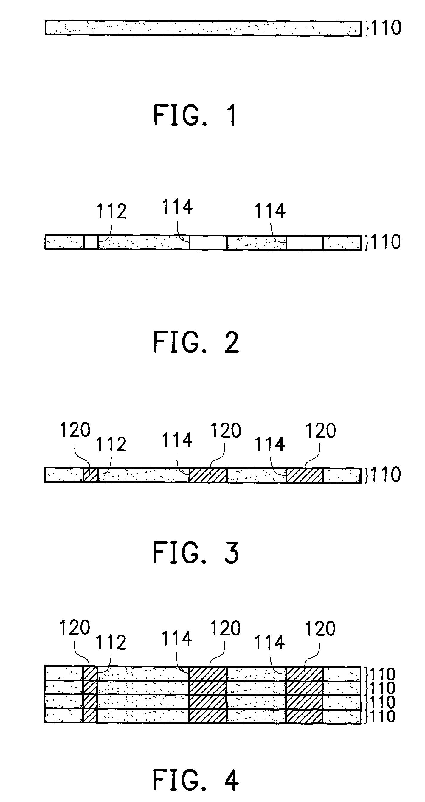
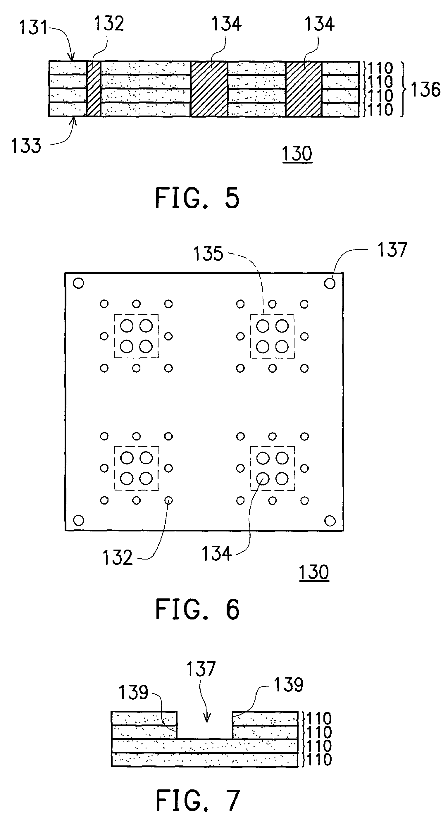
[0019]FIGS. 1–12 illustrate magnified cross-sectional views of fabricating a ceramic substrate with a thermal conductive plug in accordance with a preferred embodiment of the present invention. Referring to FIG. 1, a plurality of green tapes 110 are provided (only one of the green tapes 110 is shown in FIGS. 1–3). The green tape 110 is made of materials consisting of low temperature glass, ceramic power, a dispersant and an adhesion. The dispersant is a material used for preventing the low temperature glass and the ceramic power from agglomerating together. The adhesion is a material used for making the green tape 110 to be adhesive.

[0020]Referring to FIG. 2, a plurality of conductive openings 112 (only one is shown in the FIGS. 2–4) and a plurality of thermal conductive openings 114 are formed on the green tape 110 by utilizing a machine pouching method. A maximum width of the conductive opening 112 is approximately between 5 milli-inches to 15 milli-inches, and a maximum width of ...


PUM

PropertyMeasurementUnit
Electrical conductoraaaaaaaaaa
Widthaaaaaaaaaa
Thermal conductivityaaaaaaaaaa

Abstract

A method of fabricating a thermal conductive plug of a ceramic substrate of a multi-chip package. A plurality of conductive openings and thermal conductive openings are formed on green tapes. A metal paste is filled into the conductive openings and the thermal conductive openings. The green tapes are stacked together so that the metal paste inside the conductive openings and the thermal conductive openings of every green tape is in contact respectively with its neighboring metal paste within the conductive openings and thermal conductive openings of the green tapes. Cofire those green tapes and the metal paste to form a pre-substrate. The pre-substrate comprises an insulating structure, a plurality of thermal conductive plugs and conductive plugs.

Description

BACKGROUND OF THE INVENTION[0001]1. Field of Invention[0002]The present invention relates generally to a method of fabricating a ceramic substrate with a thermal conductive plug of a multi-chip package. More particularly, the present invention relates to a method of improving the fabricating process of the thermal conductive plug in the ceramic substrate in order to increase performance of the ceramic substrate of a multi-chip package.[0003]2. Description of the Related Art[0004]The demand of advanced electronic technology requires electronic products to be made lighter, thinner, faster, and smarter while simultaneously making them more friendly, powerful, reliable, robust, and less expensive. Thus, the trend for electronic packages is to develop highly-integrated packaging structures. Various techniques have been developed for having a large number of input / output points (I / O) in a device. The ceramic substrate is being widely utilized due to the desirable properties. Because the c...

Claims


Application Information

Patent Timeline
IPC IPC(8): H05K3/36H01L21/48H01L23/367H05K1/02H05K1/03H05K1/09H05K3/40H05K3/46
CPCH01L21/4857H01L24/32H05K1/0206H05K3/4629H05K3/4679H01L23/3677Y10T29/49155H01L2224/32057H01L2224/32225H01L2224/83385H01L2224/92247H01L2924/01027H01L2924/01029H01L2924/01047H01L2924/01079H01L2924/01082H01L2924/09701H01L2924/15787H05K1/0306H05K1/092H05K3/4053H05K3/4605H05K2201/0317H05K2201/09063H05K2203/166H01L2924/01033Y10T29/4913Y10T29/49156Y10T29/49165Y10T29/49169Y10T29/49128Y10T29/49126H01L2924/12042
Inventor HORNG, GWO-JIKUO, JEN-IHSIAU, FENG-GER
Owner NAT CHUNG SHAN INST SCI & TECH
Why Eureka
Try Eureka