

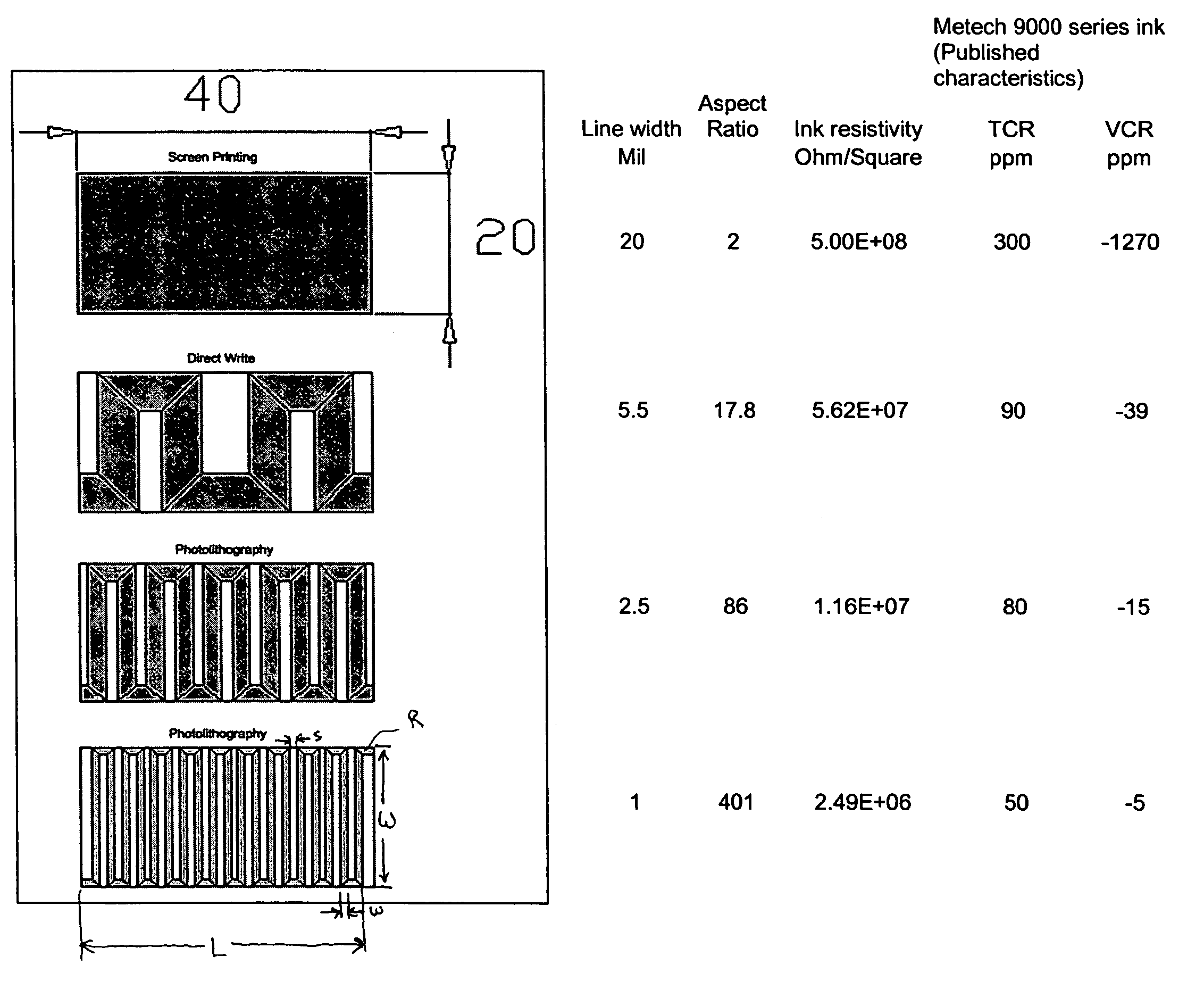
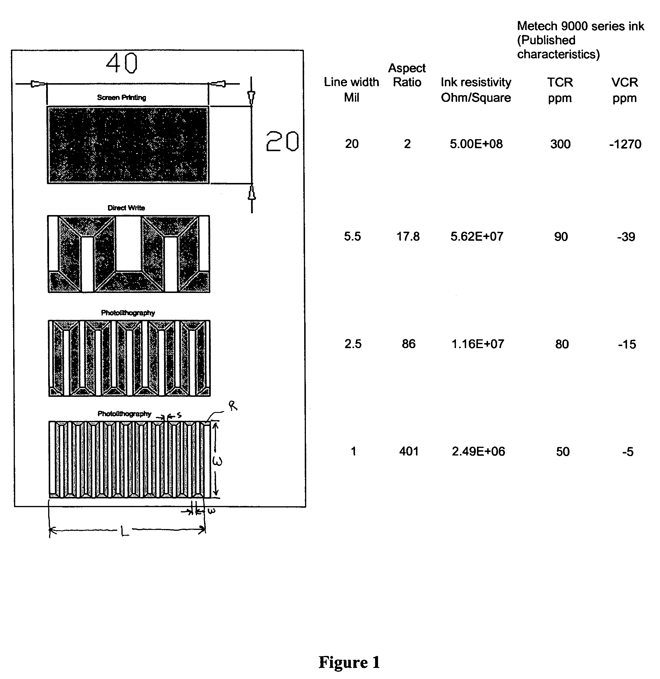
Fine line thick film resistors by photolithography
a technology of photolithography and resistors, which is applied in the direction of resistor details, printed resistor incorporation, printed electric component incorporation, etc., can solve the problems of difficult to form a continuous matrix of glass, low proportion of glass phase, and limited thin film elements, so as to improve stability, noise reduction, power handling and vcr performance, the effect of improving stability
- Summary
- Abstract
- Description
- Claims
- Application Information
AI Technical Summary
Benefits of technology
Problems solved by technology
Method used
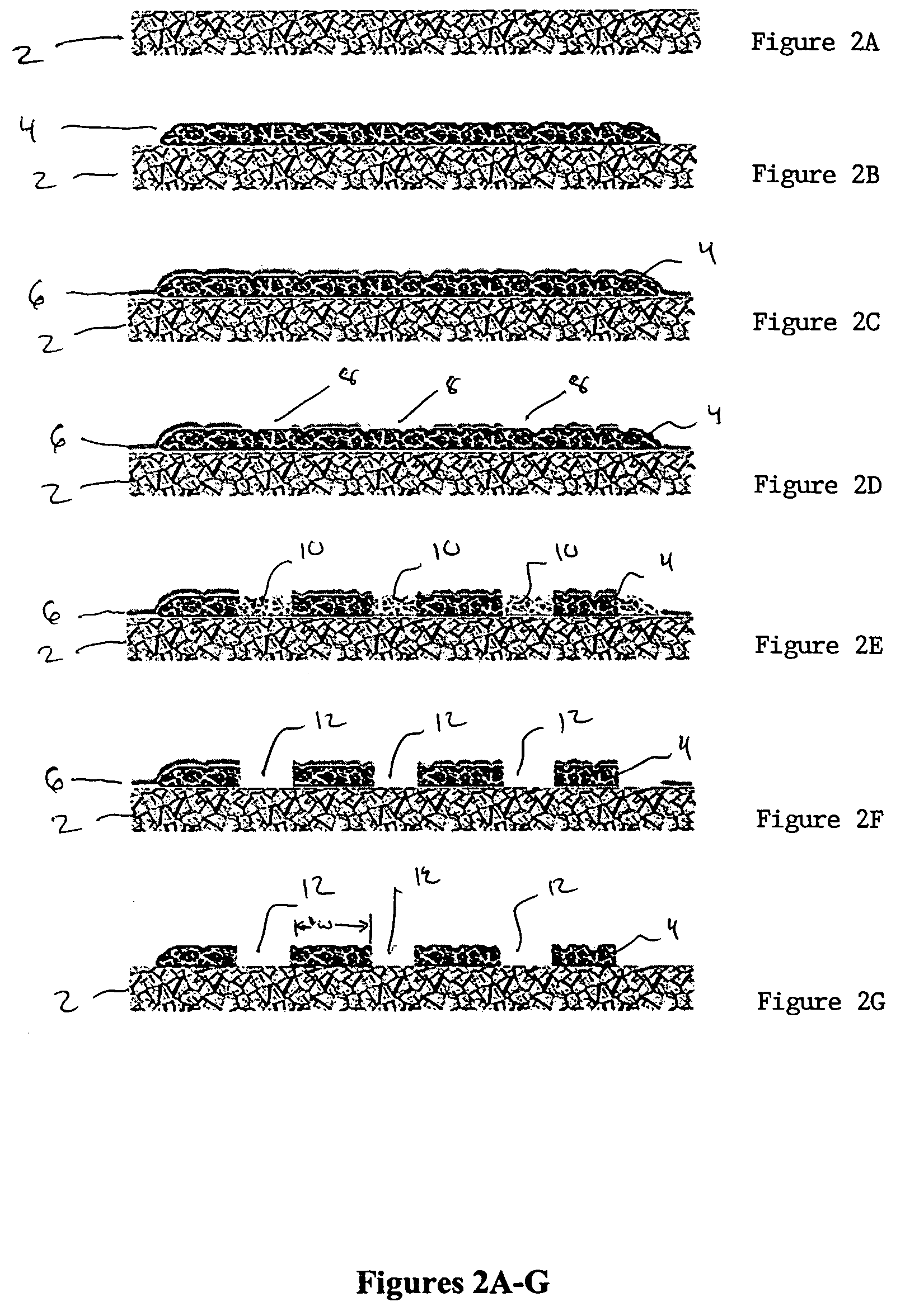
Image

Examples
example 1
Method for Fabrication
[0051]A uniform thickness of Kamaya RLP-3108 thick film resistor ink is applied to a 99.6 wt % alumina substrate by screen printing a 3 inch square block on a 3.5 inch square substrate. The ink is then dried and fired in accordance with Kamaya recommendations for temperature profile and gas environment.
[0052]A layer of AZ1518 photoresist is applied by spin coating over the film of resistor ink at 1500 RPM in an SCS Model 6708D 8″ Desk-Top Precision Spin Coating System and prebaked on a Corning hotplate for 60 seconds at 90° C.
[0053]The resist coated substrate is covered with a photomask having transparent regions in areas where the thick film will be etched away. The masked substrate is exposed in an ABM Mask aligner for 10 seconds at 1000 Watts, an intensity of 45 mW / cm2. This imagewise exposure is followed by a post exposure bake on a Corning hotplate for 60 seconds at 90° C. The cooled substrate is developed in AZ 300MIF Developer for 33 seconds at room temp...
example 2
Method for Fabrication
[0061]A uniform thickness of Kamaya RLP-3109 thick film resistor ink is applied to a 96 wt % alumina substrate by screen printing a 3 inch square block on a 3.5 inch square substrate. The ink is then dried and fired in accordance with Kamaya recommendations for temperature profile and gas environment.
[0062]A layer of AZ1518 photoresist is applied by spin coating over the film of resistor ink at 1500 RPM in an SCS Model 6708D 8″ Desk-Top Precision Spin Coating System and prebaked on a Corning hotplate for 60 seconds at 90° C.
[0063]The resist coated substrate is covered with a photomask having transparent regions in areas where the thick film will be etched away. The masked substrate is exposed in an ABM Mask aligner for 10 seconds at 1000 Watts, an intensity of 45 mW / cm2. This imagewise exposure is followed by a post exposure bake on a Corning hotplate for 60 seconds at 90° C. The cooled substrate is developed in AZ 300MIF Developer for 33 seconds at room temper...
PUM
| Property | Measurement | Unit |
|---|---|---|
| thickness | aaaaa | aaaaa |
| width | aaaaa | aaaaa |
| thickness | aaaaa | aaaaa |
Abstract
Description
Claims
Application Information