[0006]Therefore, the image sensor also need not output data for anymore than five or six frames per second to match the transfer rate. Then, it is conceivable to reduce the number of frames by lowering the operational frequency of the camera
system. As this can reduce the
power consumption by the image sensor and the
signal processing circuit, curtailment of the number of frames is an effective approach to apparatuses with a keen requirement for
power saving, such as a mobile telephone.
[0008]An object of the present invention, attempted in view of the problem noted above, is to provide a technique for making it possible to reduce the power consumption by an image
sensor system using a CMOS image sensor without adversely affecting the
image quality by lowering the frame processing speed.
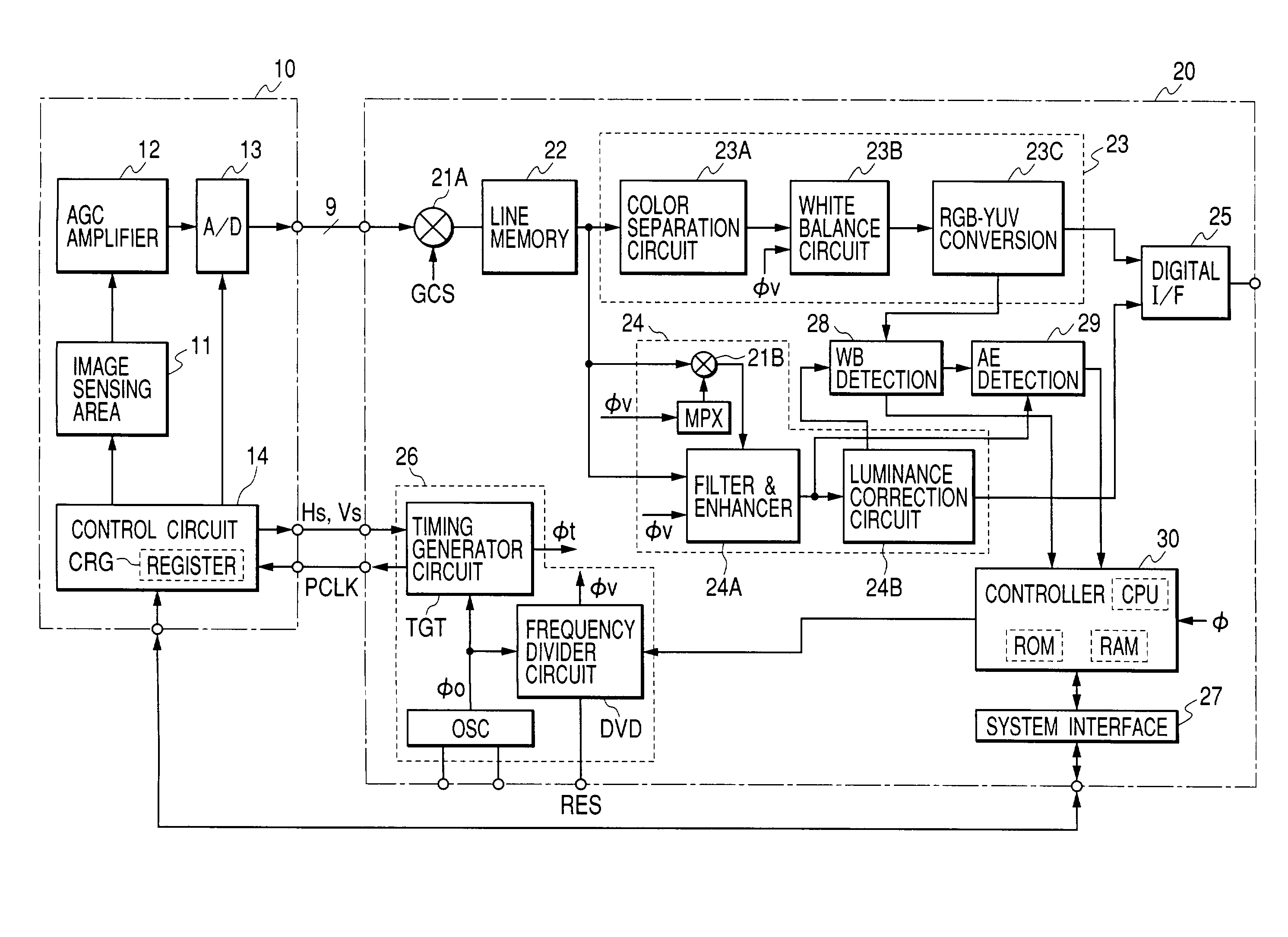
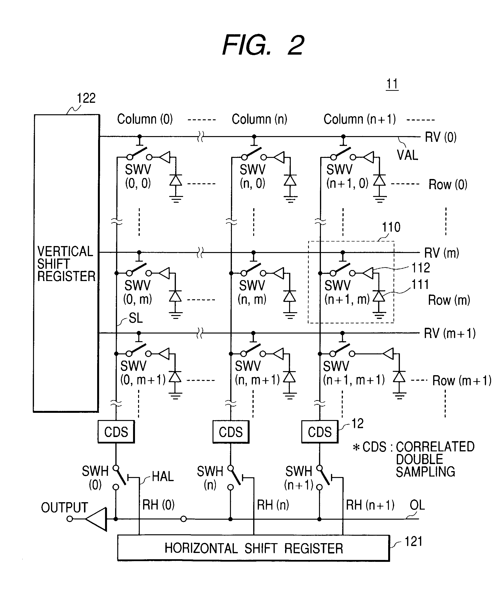
[0012]Thus, in an image sensor
system using a CMOS image sensor according to the invention, while the CMOS image sensor is operated at the full frame rate all the time, a circuit for processing image signals from the CMOS image sensor is operated at a speed close to that of full frame processing only when the power supply is turned on or when the
image sensing ambience varies and switched to a lower frame processing speed when automatic controls, including iris control, have become stabilized. In this way, power consumption can be reduced without adversely affecting image quality.
[0014]By contrast, if the present invention is applied, as the CMOS image sensor is operated at the full frame rate, such as 15 fps, when the power supply is turned on or when the image sensing ambience varies, automatic controls including iris control converge in 0.5 second or so, and by operating the sensor after that at a low rate of 3 to 7.5 fps, for instance, the power consumption can be reduced to somewhere between ½ and ⅕ of that during normal operation. On the other hand, since human operation of a camera usually takes a few seconds to dozens of seconds at a time and therefore the image sensing ambience varies at intervals of a few seconds to dozens of seconds, presumably longer than the 0.5 second taken by
automatic control by 10 times or even more, the total power consumption can be substantially reduced without sacrificing the image quality required of the camera. Furthermore, because no additional device such as a memory is needed, not only the consumption of power by the memory is absent but also there is no addition to the hardware cost.
[0015]Conceivable methods for reducing the frame processing speed of the circuit for processing image signals include one of providing on the same
semiconductor chip as the
image signal processing circuit a
frequency divider circuit capable of dividing the frequency of a reference
clock signal into a plurality of steps and reducing the frequency of the operational
clock of the
image signal processing circuit by varying the frequency division ratio of that
frequency divider circuit. As the operational
clock for the CMOS image sensor, the reference clock of the
frequency divider circuit is supplied. This facilitates synchronization between the CMOS image sensor and the
image signal processing circuit.
[0016]Further according to the invention, besides operating the CMOS image sensor at its
normal rate when the power supply is turned on or when the image sensing ambience varies, the circuit for processing image signals from the CMOS image sensor is operated at a speed matching the same frame rate as that of the image sensor and, when the
illuminance of the object is low and the image sensing ambience varies a little, the CMOS image sensor is operated at a lower frame rate than the normal, with the frame processing speed of the image
signal processing circuit also being switched to a lower rate. This makes it possible to keep the duration of accumulation of electric charges of pixels longer than the period of time taken by a full round of scanning all the horizontal scanning lines, and thereby to provide bright enough images.
