

Functional device, electrochromic device, optical device, and image-taking unit
a technology of electrochromic devices and optical devices, applied in the direction of camera filters, instruments, transportation and packaging, etc., can solve the problems of not always satisfactory method of flat band potential control, semiconductor materials of no use, and inability to prevent inverse curren
- Summary
- Abstract
- Description
- Claims
- Application Information
AI Technical Summary
Benefits of technology
Problems solved by technology
Method used
Image

Examples
example 1
[0157]Polyethylene glycol (molecular weight, 20,000) was added to an aqueous dispersion of tin oxide having a mean diameter of 5 nm, and uniformly stirred to prepare a coating liquid. For the substrate to be coated, herein used was an antireflection film-coated ITO conductive glass sheet (thickness, 0.7 mm). The coating liquid was uniformly applied onto the ITO film of the transparent conductive glass sheet. After coated, this was heated up to 450° C., taking 100 minutes, and then baked at 450° C. for 30 minutes to remove the polymer. The coating and baking was repeated until the overall coating amount of tin oxide could be 7 g / m2, and a tin oxide nano-porous electrode having a uniform thickness was thus obtained. The electrode thus formed according to the method as above had a surface roughness factor of about 400.
[0158]An electrolytic solution was prepared by dissolving lithium perchlorate in a solvent of γ-butyrolactone in an amount of 0.2 mol / liter. A compound of No. 1 to No. 11...
example 2
[0162]A method of fabricating a sample 202 (the invention) of the electrochromic device of the invention and that for a sample 201 (comparative sample) are described.
(1) Fabrication of Sample 201 (Comparative Example):
[0163]A sample 201 (comparative example) was fabricated according to a method comprising (i) coating with tin oxide nanoparticles for cathode, (ii) coating with tin oxide nanoparticles for anode, (iii) adsorption of electrochromic dye, and (iv) assembling into electrochromic device in that order.
(i) Coating with Tin Oxide Nanoparticles for Cathode:
[0164]Polyethylene glycol (molecular weight, 20,000) was added to an aqueous dispersion of tin oxide having a diameter of about 40 nm, and uniformly stirred to prepare a coating liquid. For the substrate to be coated, herein used was an antireflection film-coated ITO conductive glass sheet (thickness, 0.7 mm). The coating liquid was uniformly applied onto the ITO film of the transparent conductive glass sheet in such a manner...
example 3
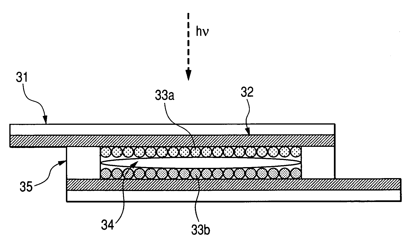
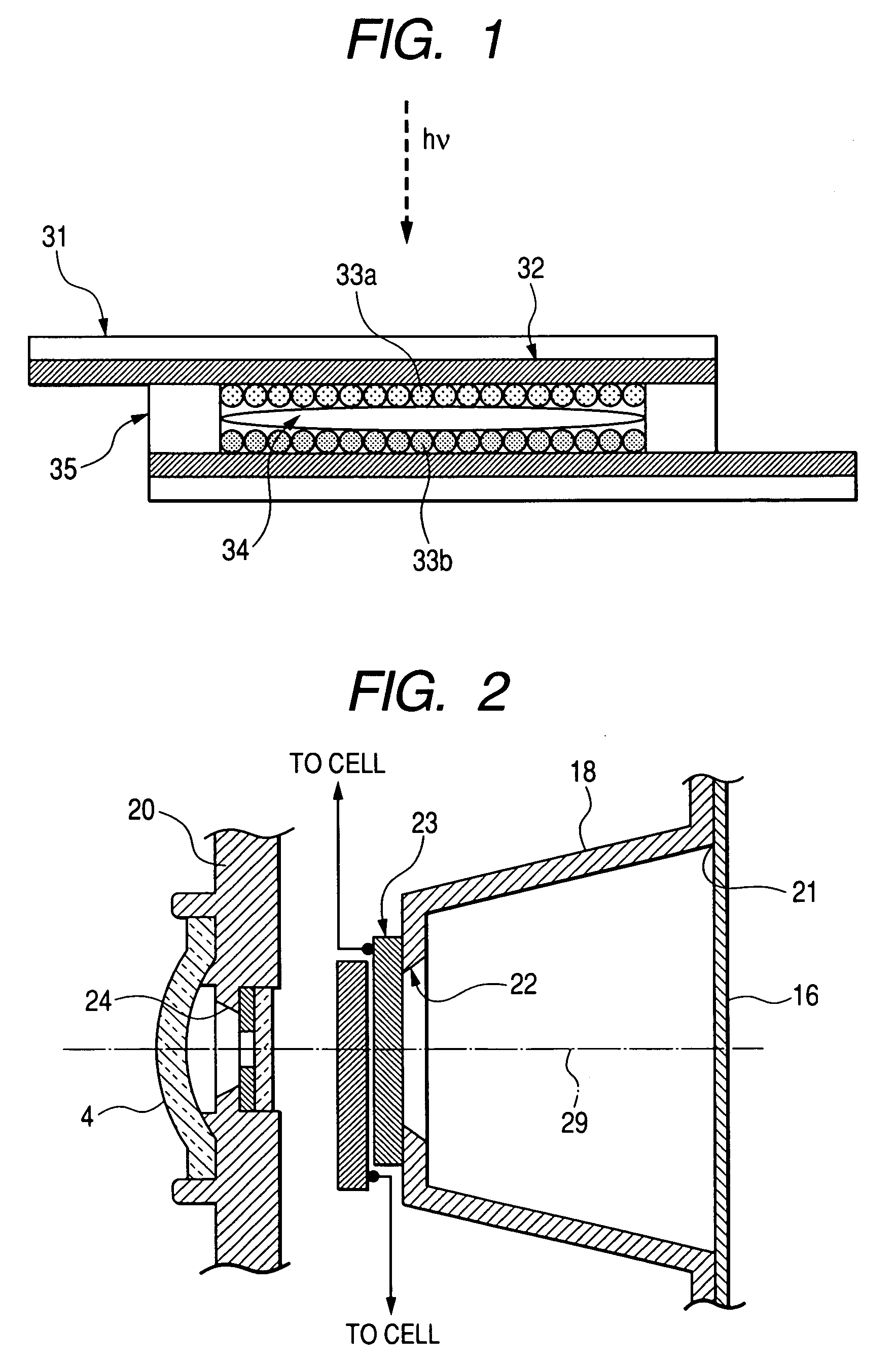
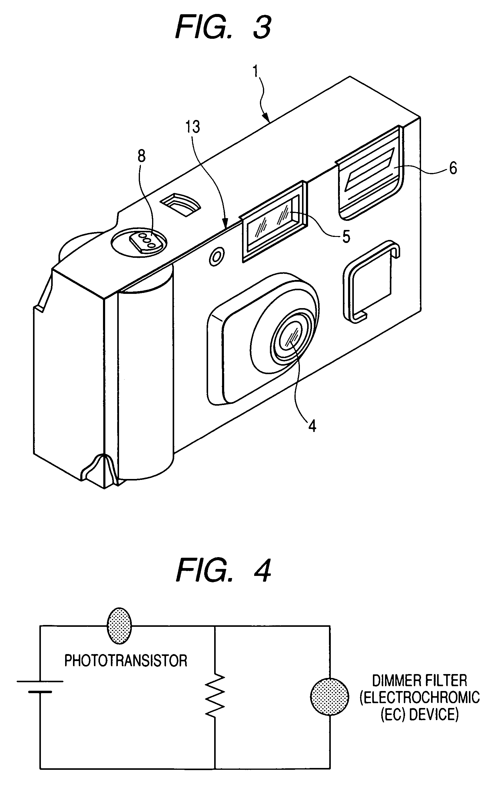
[0174]This is to demonstrate an embodiment of the electrochromic device sample 202 of the invention mounted on a lens-combined film unit.
[0175]The lens-combined film unit of this embodiment comprises (1) a dimmer filter 23 (electrochromic device) and (2) a phototransistor 13 (electromagnetic wave sensor) mounted therein, as in FIG. 2 and FIG. 3. The phototransistor 13 was disposed on the outer part of the unit. Accordingly, an electromotive force could be generated in accordance with the intensity of the external light around the device, and via the dimmer filter 23 as colored by the electromotive force, the quantity of light to reach the color negative film 16 could be controlled.
(1) Electrochromic Device Sample 202:
[0176]The electrochromic device sample 202 fabricated in Example 2 was used.
(2) Circuit of Electrochromic Device:
[0177]A phototransistor (Sharp's PT380) was used as an electromagnetic wave sensor; and as an electromotive force-generating element, used was a dry cell for...
PUM
| Property | Measurement | Unit |
|---|---|---|
| energy level | aaaaa | aaaaa |
| energy level | aaaaa | aaaaa |
| optical density | aaaaa | aaaaa |
Abstract
Description
Claims
Application Information