Method for fabricating tandem thin film photoelectric converter

a technology of tandem-type and photoelectric conversion, which is applied in the manufacture of final products, basic electric elements, climate sustainability, etc., can solve the problems of light absorbed by these inactive layers, the characteristics of the resulting tandem-type thin film photoelectric conversion device deteriorate as compared to that of a tandem-type thin film photoelectric conversion device, etc., to achieve the effect of minimizing the reduction of photoelectric conversion efficiency

Inactive Publication Date: 2007-07-03
KANEKA CORP
View PDF14 Cites 38 Cited by
  • Summary
  • Abstract
  • Description
  • Claims
  • Application Information

AI Technical Summary

Benefits of technology

[0014]In view of the circumstances of the conventional arts, the invention is aimed at to minimize the reduction in photoelectric conversion efficiency of a tandem-type thin film photoelectric conversion device due to exposure to the air when a substrate having one or more photoelectric conversion units is once taken out to the air from a deposition apparatus in mid-course of formation of a plurality of the units involved in the photoelectric conversion unit.

Problems solved by technology

However, these conductive layers are inactive layers which do not directly contribute to photoelectric conversion.
That is, light absorbed by these inactive layers is a loss, which does not contribute to electric power generation.
However, the inventors experienced that, when a first photoelectric conversion unit was formed, then a substrate including the unit was once taken out to the air from a deposition apparatus, and a second photoelectric unit was stacked thereafter, characteristics of the resulting tandem-type thin film photoelectric conversion device deteriorate as compared to that of a tandem-type thin film photoelectric conversion device wherein all units were continuously formed without taking a substrate out to the air.

Method used


Image

  • Method for fabricating tandem thin film photoelectric converter
  • Method for fabricating tandem thin film photoelectric converter
  • Method for fabricating tandem thin film photoelectric converter

Examples


example 1

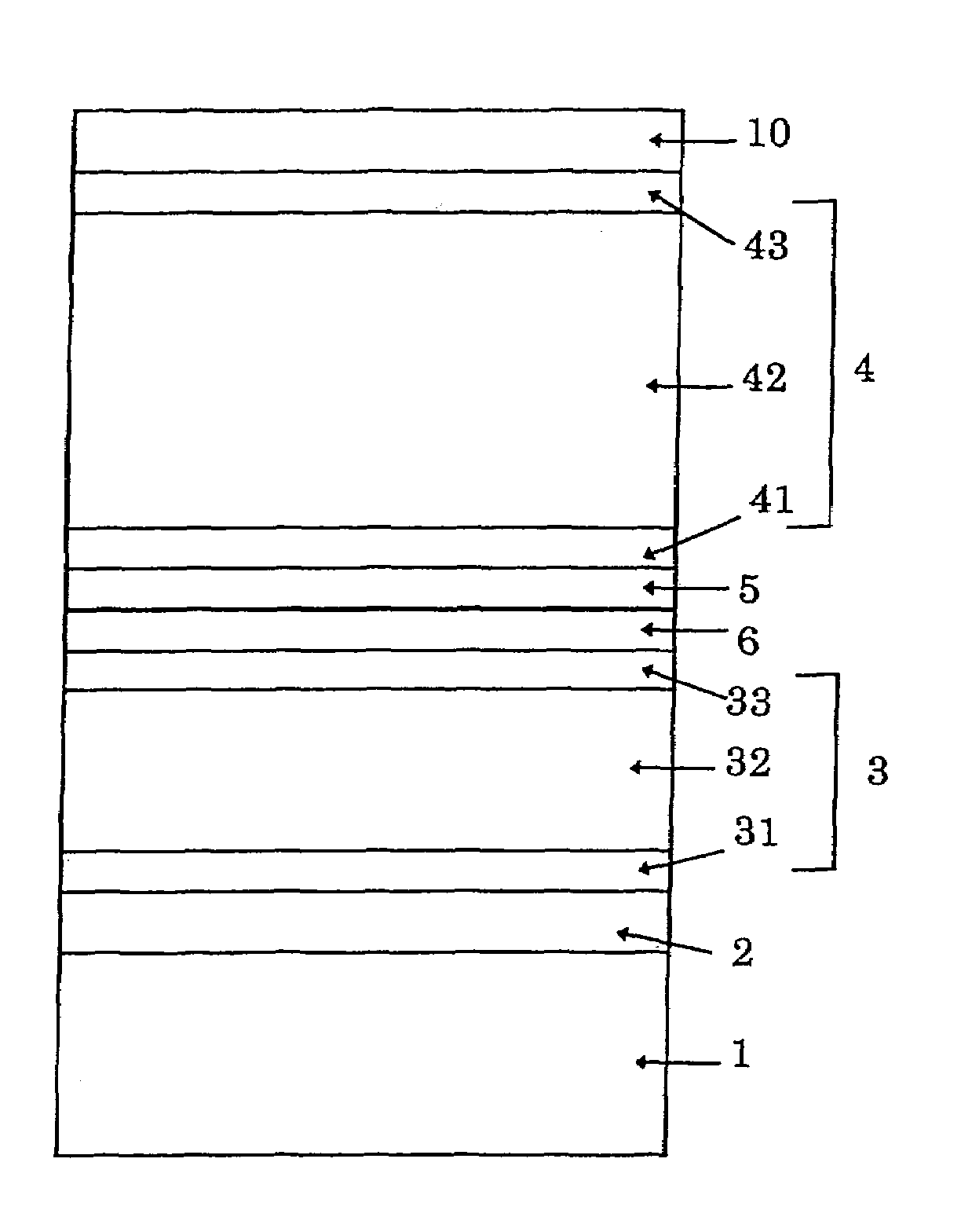
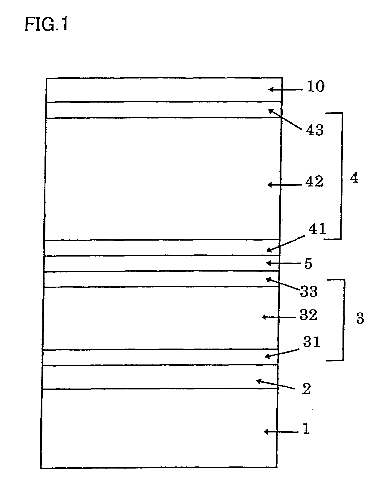
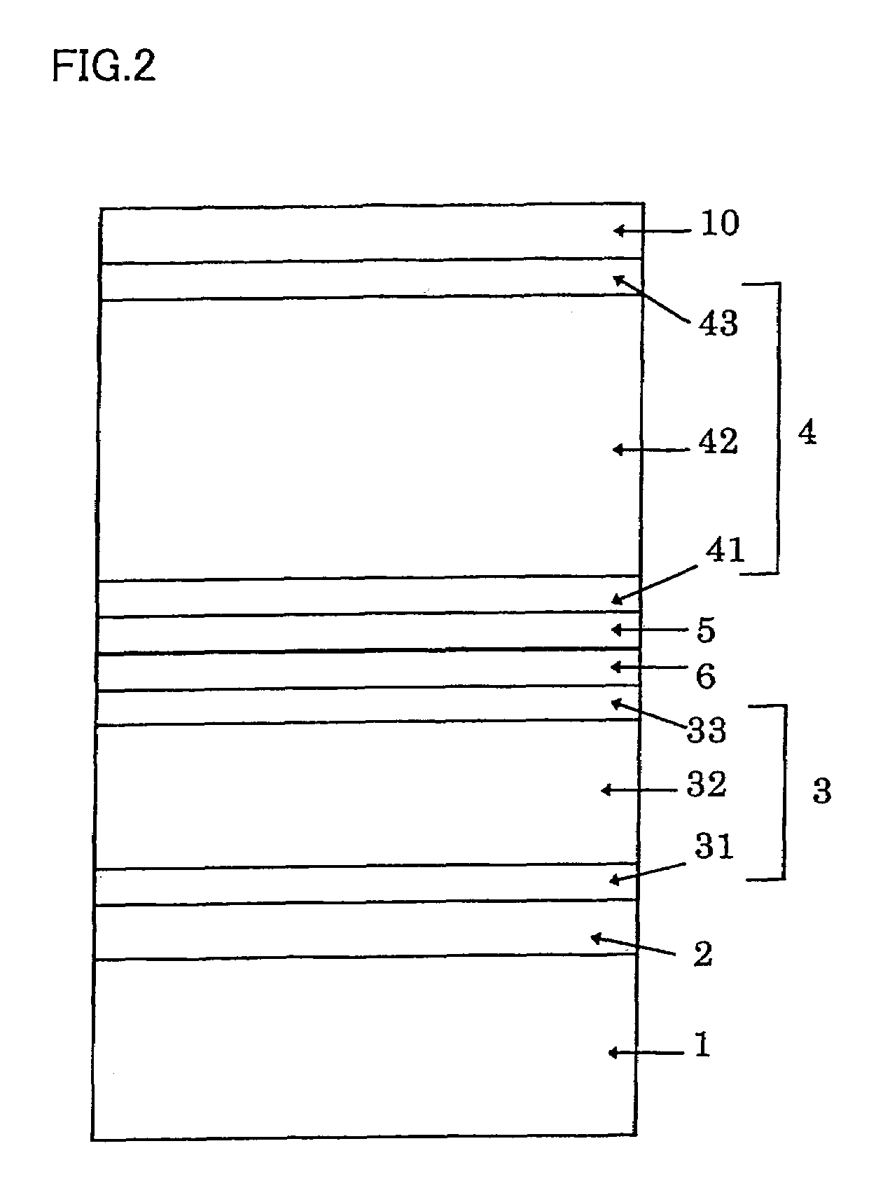
[0043]Example 1 corresponds to a method of manufacturing a thin film solar cell in FIG. 2. First of all, a transparent electrode layer 2 containing tin oxide as a main component was formed on a transparent glass substrate 1. Then, the laminate including the substrate 1 and the electrode layer 2 was introduced in a first plasma CVD apparatus, and a p-type amorphous silicon carbide layer 31, an i-type amorphous silicon photoelectric conversion layer 32 and an n-type microcrystalline silicon layer 33 included in an amorphous silicon unit 3 were formed in the thickness of 8 nm, 300 nm and 10 nm, respectively, at a predetermined substrate temperature. After the formation of the n-type layer 33, introduction of phosphine as doping gas was shut off in the same reaction chamber, and a non-doped intermediate layer 6 was formed in the thickness of 4 nm.

[0044]After that, the laminate was transferred to an unload chamber of the first plasma CVD apparatus, and the laminate was taken out to the a...

example 2

[0054]Example 2 was different from Example 1 only in that the thickness of the n-type microcrystalline silicon layer 33 in the amorphous silicon unit 3 was increased from 10 nm to 12 nm, and thereafter the laminate was taken out from the first plasma CVD apparatus to the air without formation of the non-doped intermediate layer 6. In other words, Example 2 corresponds to a method of manufacturing a hybrid thin film solar cell in FIG. 1.

REFERENCE EXAMPLE

[0055]Reference Example was different from Example 2 only in that the thickness of the n-type microcrystalline silicon layer 33 was increased to 30 nm and the crystalline silicon unit 4 was subsequently formed without exposure of the laminate to the air and also without formation of the n-type intermediate layer 5.

[0056]As shown in Table 2, it is understood that the decreases in the average photoelectric conversion efficiency of the solar cells according to both of Example 1 and Example 2 fall within the range of less than 2% in compa...


PUM


Abstract

A method of manufacturing a tandem-type thin film photoelectric conversion device includes the steps of forming at least one photoelectric conversion unit (3) on a substrate (1) in a deposition apparatus, taking out the substrate (1) having the photoelectric conversion unit (3) from the deposition apparatus to the air, introducing the substrate (1) into a deposition apparatus and carrying out plasma exposure processing on the substrate (1) in an atmosphere of a gas mixture containing an impurity for determining the conductivity type of the same conductivity type as that of the uppermost conductivity type layer (33) and hydrogen, forming a conductivity type intermediate layer (5) by additionally supplying semiconductor raw gas to the deposition apparatus, and then forming a subsequent photoelectric conversion unit (4).

Description

TECHNICAL FIELD[0001]The present invention relates to a method of manufacturing a tandem-type thin film photoelectric conversion device and, more particularly, to a method of manufacturing which can suppress reduction in performance of a photoelectric conversion device, enhance the flexibility of manufacturing steps and improve manufacturing efficiency. In the specification, terms “crystalline” and “microcrystalline” are used also for a state partially including amorphous regions, as generally used in the field of the art.BACKGROUND ART[0002]In recent years, semiconductor thin film photoelectric conversion devices as represented by a solar cell have been diversified, and crystalline silicon thin film solar cells have been developed in addition to conventional amorphous silicon thin film solar cells. Furthermore, a tandem (hybrid)-type thin film solar cell having a stack thereof have come into practical use.[0003]In general, a silicon thin film photoelectric conversion device include...

Claims


Application Information

Patent Timeline
Patent Type & Authority Patents(United States)
IPC IPC(8): H01L21/00H01L31/04H01L31/075H01L31/06H01L31/076H01L31/077H01L31/20
CPCH01L31/076H01L31/202Y02E10/548Y02E10/547Y02P70/50H01L31/075
Inventor YOSHIMI, MASASHISUEZAKI, TAKASHIYAMAMOTO, KENJI
Owner KANEKA CORP
Why Eureka
Try Eureka