Controlled nanowire growth in permanent, integrated nano-templates and methods of fabricating sensor and transducer structures

a technology of integrated nano-templates and controlled nanowires, which is applied in the direction of nanostructured devices, nanoinformatics, coatings, etc., can solve the problems of difficult electrical contact, complex process, and difficult to assemble wires into rational device geometries

Inactive Publication Date: 2007-07-03
PENN STATE RES FOUND
View PDF5 Cites 38 Cited by
  • Summary
  • Abstract
  • Description
  • Claims
  • Application Information

AI Technical Summary

Benefits of technology

[0017]An advantage of the present invention is to create permanent nanotemplates which control nanostructure growth and also become part of the overall device or array (or both) structure. The techniques of the invention using VLS / integrated, permanent template approach for creating nanostructures such as nanowires of nanoscale diameters and nanotapes of nanoscale thicknesses overcome the disadvantages associated with disposable templates.
[0018]Another advantage of the present invention is it provides a nanostructure growth technique using nanochannel structures for contactable, dopable, straight or curved and size-controllable nanowires.
[0019]Yet another advantage of the invention is its ability to use field-augmented effects in the nanowire growth.
[0020]Still another advantage of the invention is to provide a technique described here that allows nanostructure growth to be precisely positioned and allows nanostructures to self-assemble into a device. Moreover, the nanostructures may exist in several layers also with this invention.
[0021]Yet another advantage of the invention is the elimination of a need to have only straight channels. More specifically, the channels of the invention may have branches, if advantageous to have branching nanostructures, and can have varying cross-sections. Also, if desired to be built into templates, contacts may be built-in and the fabricated nanostructures may exist on several levels and cross each other.
[0022]In yet another aspect of the present invention, a method includes forming a nanostructure including forming an insulating substrate, forming a sacrificial layer in a predetermined pattern on the substrate and forming a capping layer over at least part of the sacrificial layer, selectively removing the sacrificial layer to create a nanochannel between the capping layer and the substrate, and forming at least one nanostructure using the nanochannel region.

Problems solved by technology

It remains a challenge to grow composition-controllable, orientation-controllable and size-controllable nanowires.
It is also difficult to assemble the wires into rational device geometries and enable current flow between nanoscale and microscale structures.
The use of the alumina membranes as the templates (e.g., dissolved / etched away templates) may provide control over nanowire diameter and length while also enabling the production of single crystal material, however, there are many disadvantages to current approaches.
All of these steps use electroplating and make the process complicated;5. The alumina template is disposed of (etched away) in this approach and cannot be integrated with device assembly.
It is very difficult to separate, move, electrically contact, if needed, and assemble these freed nanowires; and6. The process is not compatible with on-chip fabrication and assembly, and requires post synthesis assembly of nanostructures to form more complicated devices.

Method used


Image

  • Controlled nanowire growth in permanent, integrated nano-templates and methods of fabricating sensor and transducer structures
  • Controlled nanowire growth in permanent, integrated nano-templates and methods of fabricating sensor and transducer structures
  • Controlled nanowire growth in permanent, integrated nano-templates and methods of fabricating sensor and transducer structures

Examples


Embodiment Construction

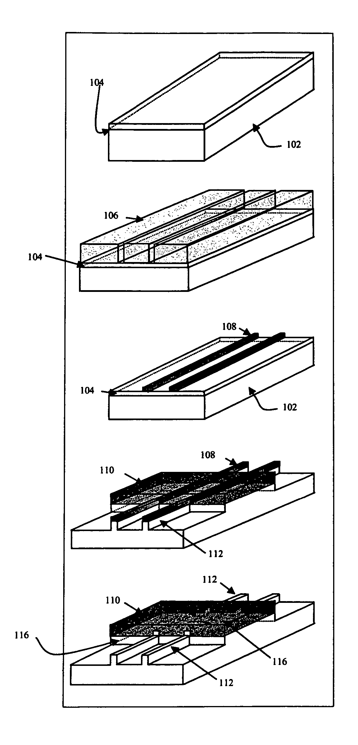
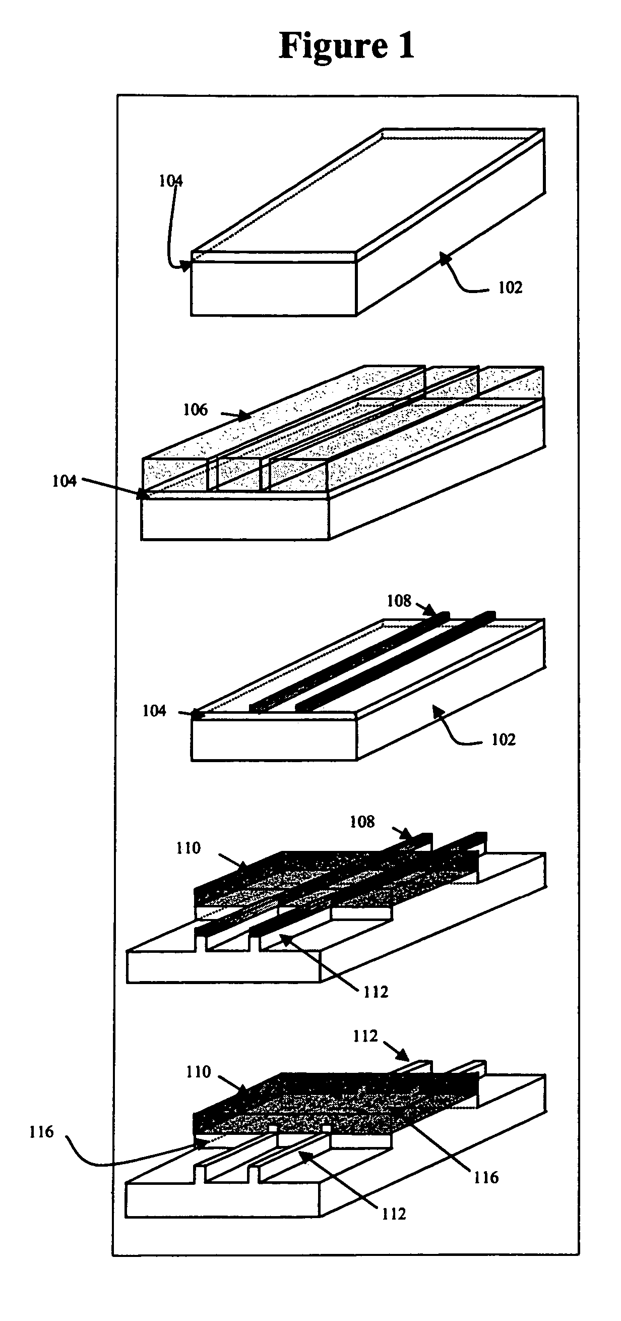
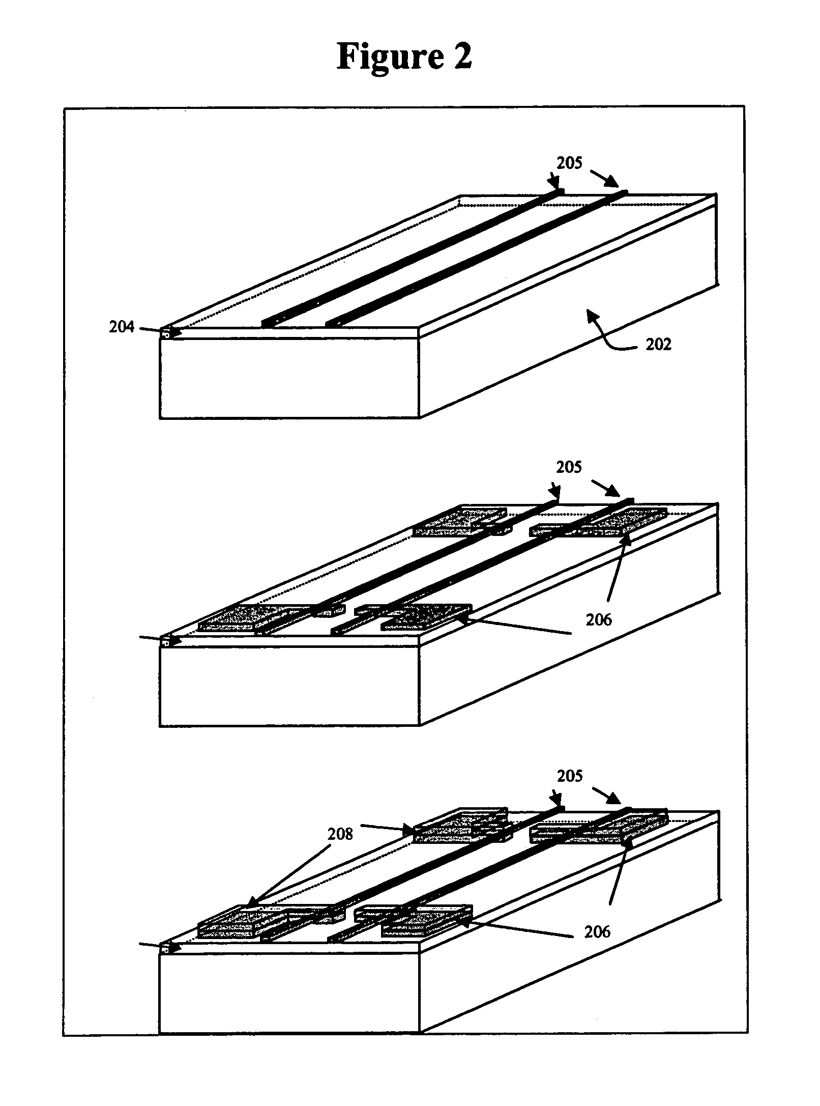
[0047]This invention presents a novel method to form uniform or heterogeneous, straight or curved and size-controllable nanostructures including, for example, nanowires, nanoribbons, nanotubes, and nanotapes (e.g., high width to height ratio cross-section) including single crystal SiNW, in a nanochannel template. In the case of semiconductor nanowires, doping can be included during growth. Electrode contacts are present as needed and may be built in to the template structure. Thus, completed devices such as diodes, transistors, solar cells, sensors, and transducers are fabricated, contacted, and arrayed as nanostructure and resultant device fabrication is completed. Optionally, the template is not removed and may become part of the structure.

[0048]Nanochannel templates are fabricated by the combined use of lithography and sacrificial material patterning techniques known in the art. The nanochannels can be straight or curved, as desired, and the sizes are controllable. Hence the nano...


PUM

PropertyMeasurementUnit
diameteraaaaaaaaaa
temperaturesaaaaaaaaaa
critical diameteraaaaaaaaaa

Abstract

This invention presents a novel method to form uniform or heterogeneous, straight or curved and size-controllable nanostructures including, for example, nanotubes, nanowires, nanoribbons, and nanotapes, including SiNW, using a nanochannel template. In the case of semiconductor nanowires, doping can be included during growth. Electrode contacts are present as needed and may be built in to the template structure. Thus completed devices such as diodes, transistors, solar cells, sensors, and transducers are fabricated, contacted, and arrayed as nanowire or nanotape fabrication is completed. Optionally, the template is not removed and may become part of the structure. Nanodevices such as nanotweezers, nanocantilevers, and nanobridges are formed utilizing the processes of the invention.

Description

RELATED APPLICATION DATA[0001]This application claims the benefit of U.S. Provisional Patent Application No. 60 / 528,487, filed on Dec. 11, 2003, which is hereby incorporated by reference for all purposes as if fully set forth herein.BACKGROUND OF THE INVENTION[0002]1. Field of the Invention[0003]The present invention relates to a method to form uniform or heterogeneous, straight or curved and size-controllable nanostructures using nanochannel templates. More specifically, this method may be used to form devices and systems utilizing nanowires.[0004]2. Discussion of the Related Art[0005]One-dimensional metallic and semiconducting nanowires have attracted much attention recently owing to their fundamental and technological importance. Much of this attention is focused on Si nanowires (SiNW) since, at this scale, Si can become a direct-band-gap material. In the article, by B. Marsen, et al., “Fullerene-Structured Nanowires of Silicon,” Phys. Rev., V. 60, No. 16 (1999), it was suggested...

Claims


Application Information

Patent Timeline
Patent Type & Authority Patents(United States)
IPC IPC(8): H01L21/36H01L21/20B81C1/00H01L21/44H01L29/06H01L51/00
CPCB81C1/0019B82Y10/00H01L21/0237H01L21/02532H01L21/0259H01L21/02603H01L21/02639H01L21/02645H01L21/02653H01L29/0665H01L29/0673H01L29/068H01L51/0002B81B2203/0109B81B2203/0118Y10S977/762Y02E10/549H10K71/10
Inventor FONASH, STEPHEN J.SHAN, YINGHUIPENG, CHIH-YIKALKAN, ALI KAANCUIFFI, JOSEPH D.HAYES, DANIELBUTTERFOSS, PAULNAM, WOOK JUN
Owner PENN STATE RES FOUND
Why Eureka
Try Eureka