Enhanced performance mode converter

a converter and performance technology, applied in the field of optical mode converters, can solve the problems of less effective modulator, prone to problems, and ineffective electronic mode modulator

Active Publication Date: 2007-07-10
OPTELIAN ACCESS NETWORKS
View PDF14 Cites 28 Cited by
  • Summary
  • Abstract
  • Description
  • Claims
  • Application Information

AI Technical Summary

Benefits of technology

[0014]It is an object of the present invention to obviate or mitigate at least one disadvantage of previous mode converter modulators.
[0015]In a first aspect of the present invention, there is provided an optical mode converter for receiving an input light beam having an initial state of polarization (SOP) and for converting the initial SOP to a desired SOP. The optical mode converter comprises an optical guiding layer and an electrode structure. The optical guiding layer has an optical waveguide formed from an electro-optic material. The optical guiding layer and waveguide both have a layer with free carriers. The electrode structure has two electrodes. The electrodes are disposed on opposing sides of the optical waveguide and each has a conductor strip with projections that extend towards the optical waveguide. The electrode structure produces an electric field across the waveguide upon application of a voltage signal, and additionally produces both an inductance and a capacitance. Each electrode has a metal portion in contact with the layer having free carriers to form a Schottky barrier adjacent the waveguide to reduce accumulation of free carriers.
[0016]In embodiments of the present invention, the optical waveguide supports both a low order optical mode and a higher order optical mode, the higher order optical mode attenuated by the Schottky barrier and the inductance and capacitance produced by the electrodes and projections slows the propagation of the voltage signal through the electrode structure to substantially the velocity of the input light beam through the optical waveguide.

Problems solved by technology

Electro-optic mode modulators such as the ones disclosed in '257 are prone to problems caused by the presence of free carriers, i.e. conduction electrons or holes, in the semiconductor epilayer.
This accumulation of free carriers leads to a screening of the electric field in the waveguide which leads to a less effective modulator.
The screening of the electric field is most pronounced at low frequencies, making the modulator difficult to bias to a desired operating point.
Furthermore, in cases where a large biasing field is required to overcome modal birefringence between the TE and TM-like modes, the field screening problem is compounded.
Another problem with electro-optic modulators such as described in '257 is that related to the presence of higher order optical modes in the waveguide.
The presence of these higher modes lead to unpredictable behaviour depending on the amount of power coupled into the higher order modes.
Higher order modes can result in degraded extinction ratio and transfer function instability.
However, as in the case where the distance separating the pads is decreased, a higher ratio of pad length to pad pitch leads to an increase in capacitance and a decrease in impedance.
As mentioned above, the presence of free carriers in electro-optic modulators such as disclosed in '257 leads to poor device performance.
The number of free carriers generated by the two photon absorption process depends on the optical intensity becomes more problematic as the intensity of the light beam is increased.

Method used


Image

  • Enhanced performance mode converter
  • Enhanced performance mode converter
  • Enhanced performance mode converter

Examples


Embodiment Construction

[0026]The present invention sets out to provide an enhanced electro-optical mode converter by alleviating problems due to the presence of free carriers (both intrinsic free carriers and free carriers generated through multi-photon absorption) in the waveguide region of the modulator. The invention further sets out to mitigate the effect of the presence of higher order modes in the waveguide as well as to provide a means for allowing a lower mode conversion voltage without substantially augmenting the modulator's inductance and capacitance.

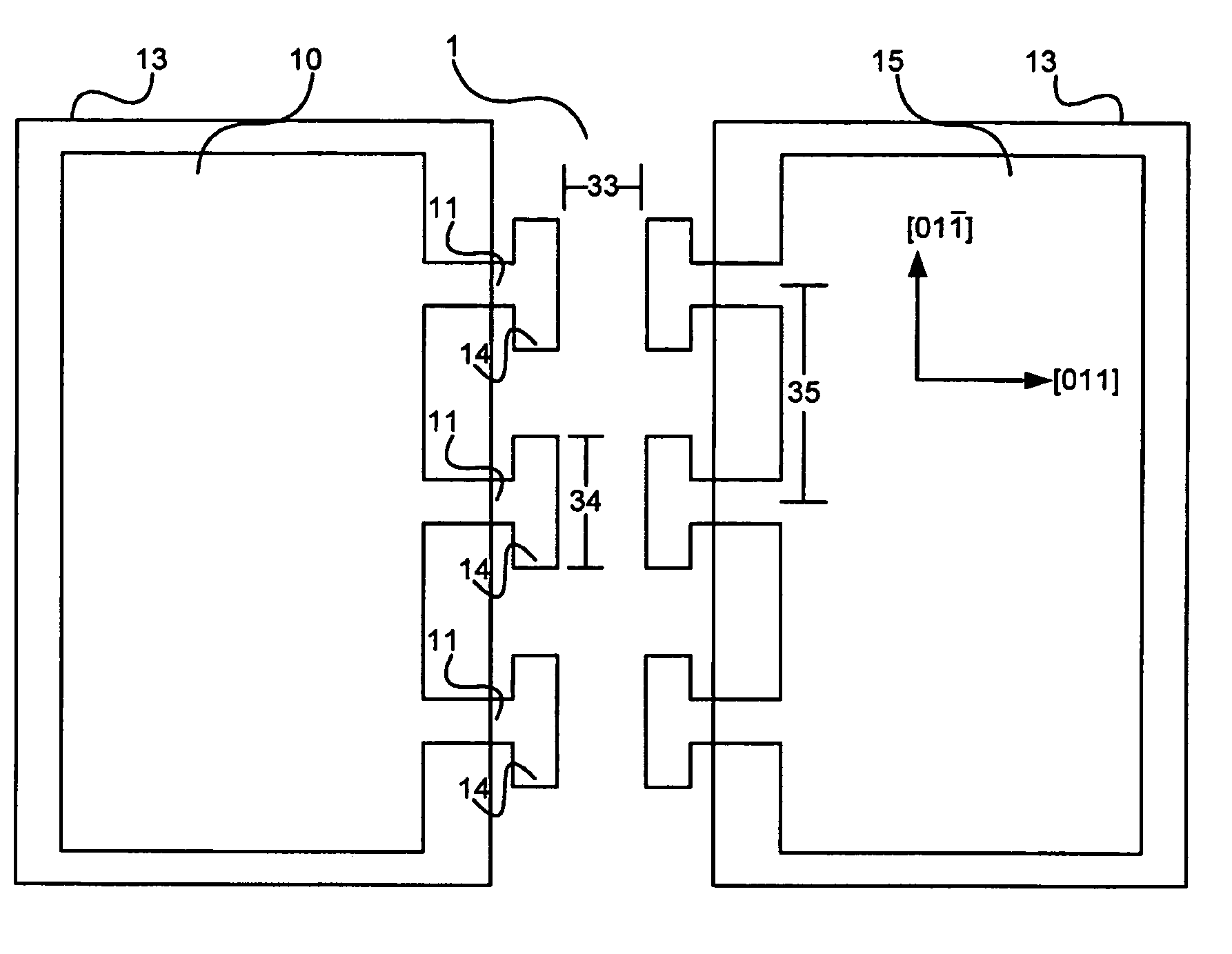
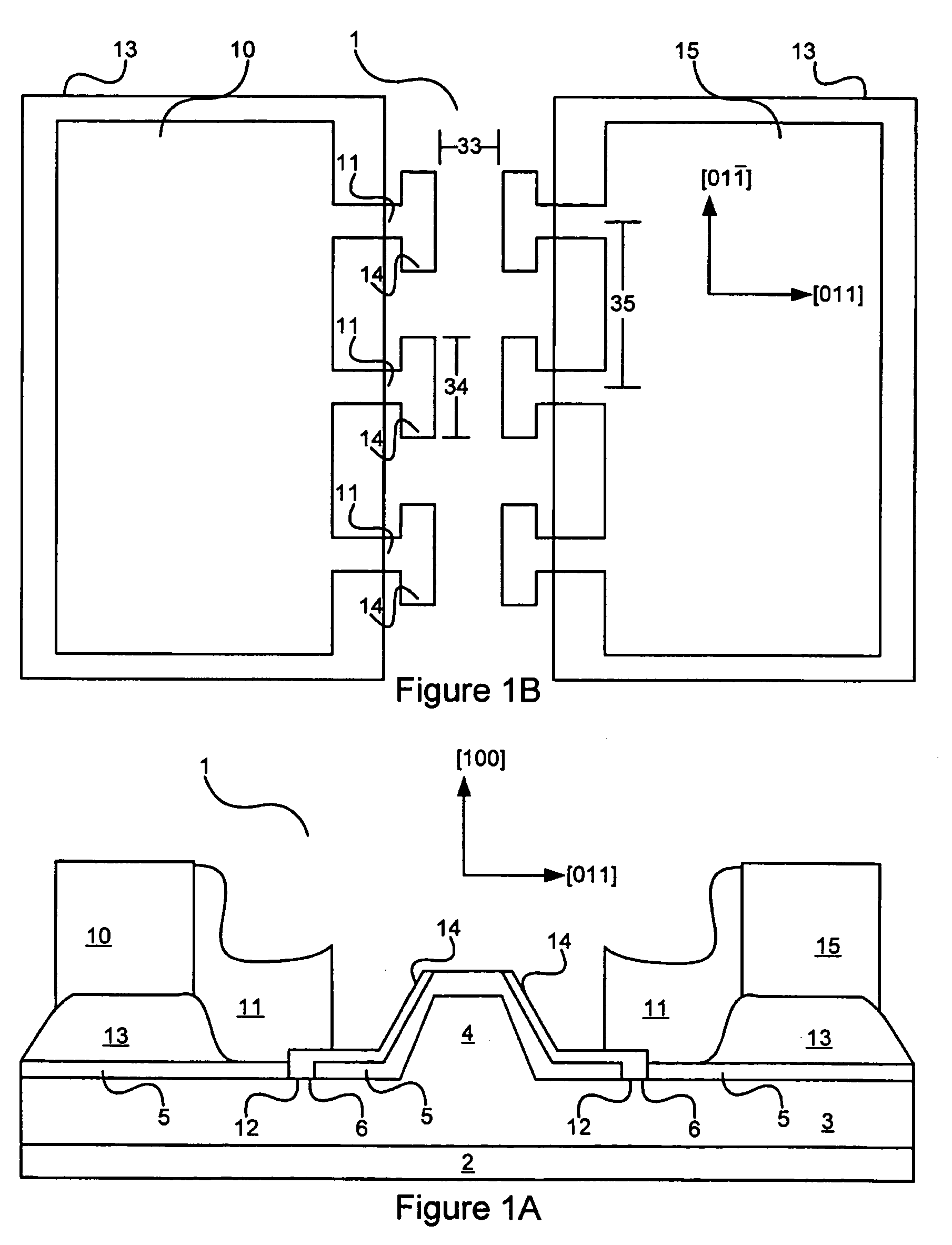
[0027]An embodiment of the present invention is shown in FIGS. 1A and 1B where cross-sectional and top views of optical mode converter 1 are respectively shown.

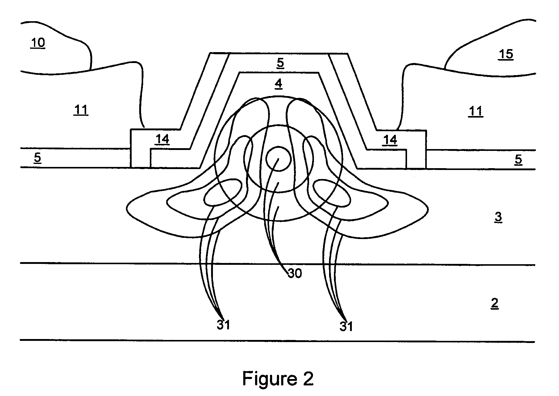
[0028]A substrate 2 supports an optical guiding layer, such as layer 3, which includes a waveguide, such as ridge optical waveguide 4. In a presently preferred embodiment, the optical guiding layer, illustrated as layer 3, is epitaxially grown on substrate 2, though in other embodiments, lay...


PUM

PropertyMeasurementUnit
impedanceaaaaaaaaaa
dielectric constantaaaaaaaaaa

Abstract

An optical mode converter comprising a slow wave electrode structure and including Schottky barriers for preventing an accumulation of free carriers in the optical waveguide region of the converter. The Schottky barriers are also used for suppressing higher order modes in the waveguide. Low refractive index insulators are used to allow efficient driving of the device without hindering the impedance or the microwave index of the optical mode converter. Two-photon absorption processes are eliminated through the use of a waveguide semiconductor material having a bandgap of at least twice the photon energy of the light beam propagating through the optical mode converter.

Description

FIELD OF THE INVENTION[0001]The present invention relates generally to optical mode converters. More particularly, the present invention relates to electro-optical mode converters having a slow wave electrode structure.BACKGROUND OF THE INVENTION[0002]Electro-optical mode converters are used in optical communications systems to allow rapid modulation of an optical signal in accordance with an electrical signal. In most cases, an input light beam having an input state of polarization (SOP) impinges on and traverses through an electro-optical waveguide subjected to an applied electric field. When the geometry of the waveguide and the applied electric field are such that the input SOP is not aligned with a principal axis of the waveguide, the light beam at the output of the waveguide will generally have an output SOP different from the input one. With proper choice of input SOP, waveguide geometry and applied electrical field, it is possible to have the output SOP orthogonal to the inp...

Claims


Application Information

Patent Timeline
Patent Type & Authority Patents(United States)
IPC IPC(8): G02B6/10G02F1/035
CPCG02B6/14G02F1/0136G02F1/035G02F2202/10
Inventor BULL, JEFFREY D.KATO, HIROSHIJAEGER, NICOLAS AUGUST FLEMINGLU, PINGHE
Owner OPTELIAN ACCESS NETWORKS
Why Eureka
Try Eureka