Systems and methods for processing a set of circuit boards

a technology of circuit board and processing method, which is applied in the direction of stacked spaced pcbs, chemistry apparatus and processes, cleaning using liquids, etc., can solve the problems of contamination posing a threat to the circuit board, the circuitry within such components is becoming increasingly sensitive to the cleanliness of the circuit board, and the above-described conventional approach to manufacturing circuit boards. achieve the effect of reducing the amount of time and energy

Active Publication Date: 2007-08-07
EMC IP HLDG CO LLC
View PDF24 Cites 18 Cited by
  • Summary
  • Abstract
  • Description
  • Claims
  • Application Information

AI Technical Summary

Benefits of technology

[0022]In some arrangements, the circuit board processing system further includes a planar-shaped barrier coupled to the wash tank, the primary rinse tank, and the secondary rinse tank. The planar-shaped barrier is configured to define at least a portion of (i) an enclosed wash tank space above the wash tank, (ii) an enclosed primary rinse tank space above the primary rinse tank, and (iii) an enclosed secondary rinse tank space above the secondary rinse tank. In these arrangements, the ventilation subassembly is configured to simultaneously draw the vapors from the enclosed wash tank space above the wash tank, the enclosed primary rinse tank space above the primary rinse tank, and the secondary rinse tank space above the secondary rinse tank. Such a configuration shields the user of the circuit

Problems solved by technology

Unfortunately, there are deficiencies to the above-described conventional approaches to manufacturing circuit boards.
Rather, even the “No Clean” fluxes and the “No Clean” solder pastes still leave at least a minimal amount of contamination on circuit boards, and such contamination poses a threat to the circuit boards over time (e.g., the wet battery effect).
In particular, as pitch/density of contacts on component packages increases and as power consumption by components increases over time, circuitry within such components have been growing increasingly sensitive to circuit board cleanliness, e.g., due to changes in surface insulation resistance (SIR).
Additionally, the “No Clean” fluxes and “No Clean” solder pastes are only suitable for use with certain types of solders and at certain temperatures.
Accordingly, if the manufacturer uses multiple soldering processes at different temperatures (e.g., to mount components to both sides of the circuit board using re-flow soldering, to mount multi-chip modules having pre-soldered components, etc.), the temperature restrictions of the “No Clean” fluxes and “No Clean” solder pastes hinder the choices of solders and soldering temperatures available to the circuit board manufacturer.
Also, any remaining “No Clean” residues tend to char and/or poorly mix with new fluxes during rework processes if performed on the circuit boards thus pos

Method used


Image

  • Systems and methods for processing a set of circuit boards
  • Systems and methods for processing a set of circuit boards
  • Systems and methods for processing a set of circuit boards

Examples


Embodiment Construction

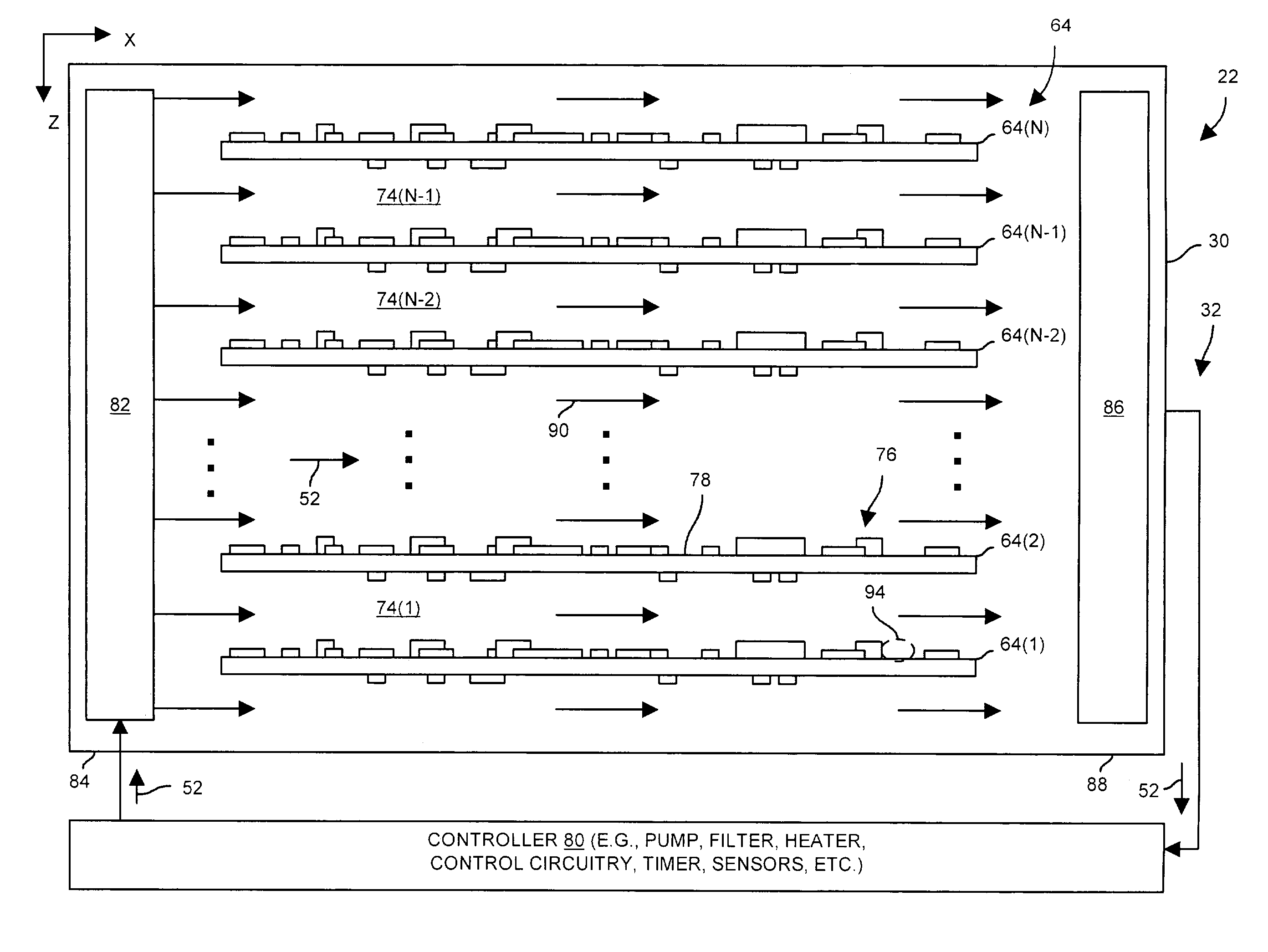
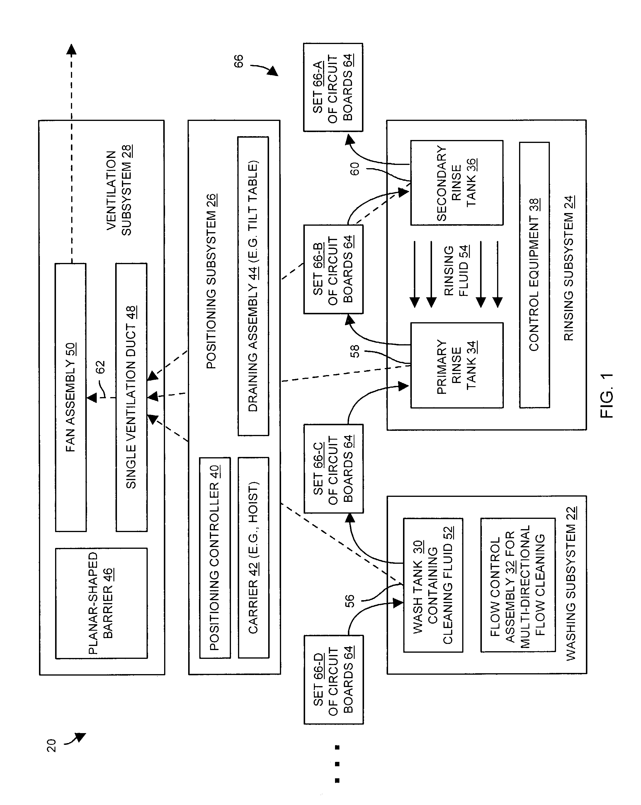
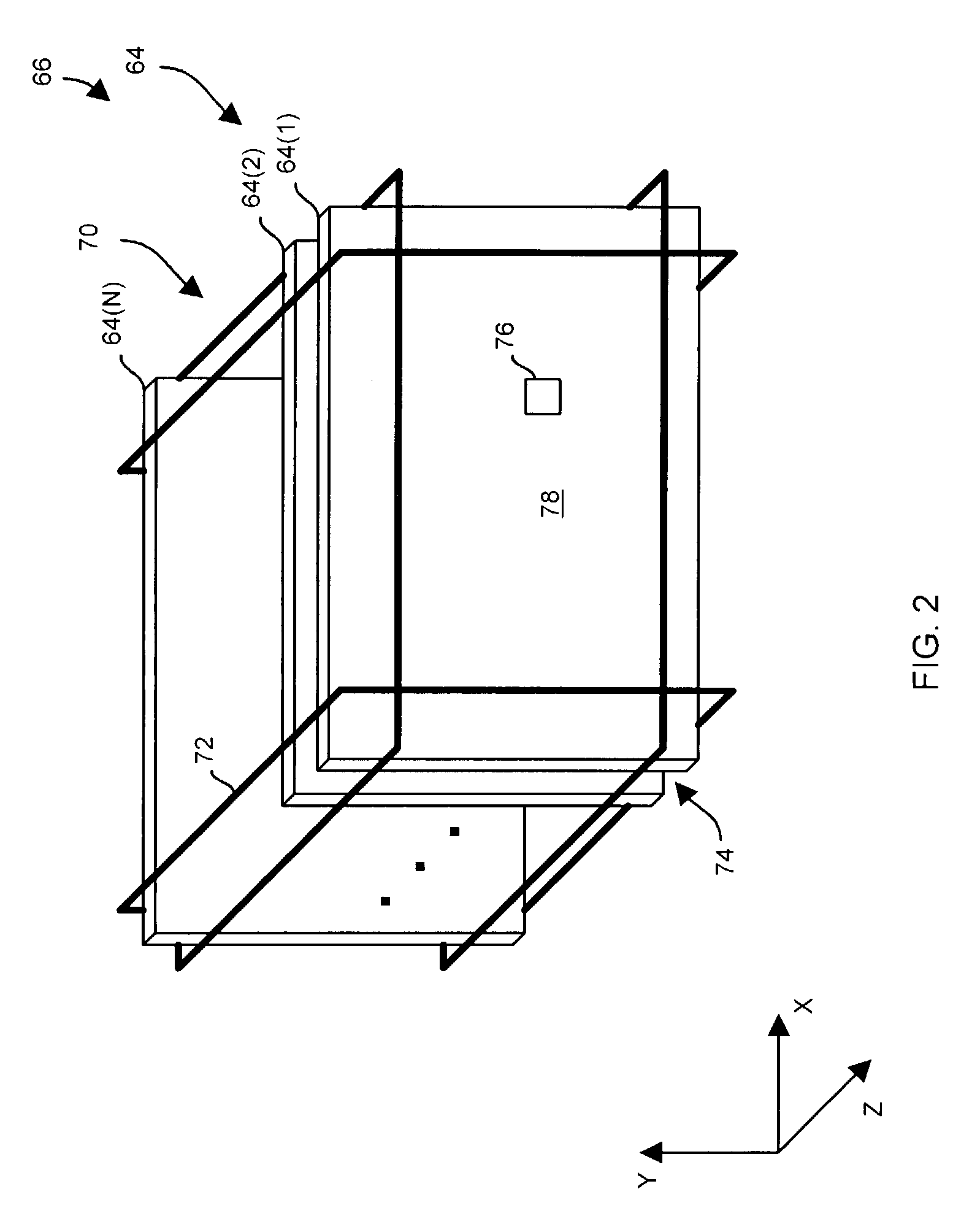
[0033]The invention is directed to circuit board processing techniques which involve cleaning circuit boards by providing a first flow of cleaning fluid (e.g., aqueous solvent) in a first direction relative to the circuit boards and subsequently a second flow of the cleaning fluid in a second direction relative to the circuit boards, while the circuit boards are immersed in a wash tank containing the cleaning fluid. The multiple flows of cleaning fluid at different times reduce or even eliminate the likelihood of forming neutral points within the tank of cleaning fluid. In particular, if the flow in the first direction results in a neutral point at a particular circuit board location, the chance is extremely remote that the flow in the second direction (e.g., a direction opposite the first direction) will form a similar neutral point at the same location. Rather, the turbulence caused by the different flows, as well as the changing of the flows in different directions, results in mo...


PUM


Abstract

A circuit board processing system includes a wash tank configured to contain cleaning fluid, and a positioning subsystem configured to immerse a set of circuit boards into the wash tank. The system further includes a flow control subsystem having (i) a first set of nozzles disposed within the wash tank, (ii) a second set of nozzles disposed within the wash tank, and (iii) a controller. The controller is configured to direct the cleaning fluid through the first set of nozzles to provide a flow of the cleaning fluid in a first direction relative to the set of circuit boards. The controller is further configured to direct the cleaning fluid through a second set of nozzles to provide a flow of the cleaning fluid in a second direction relative to the set of circuit boards after providing the flow of the cleaning fluid in the first direction.

Description

BACKGROUND OF THE INVENTION[0001]A typical circuit board manufacturing process includes a soldering stage and a cleaning stage. One type of circuit board manufacturing process involves soldering surface mount components to the surface of a bare circuit board and then cleaning the circuit board to remove contaminants. In the soldering stage of this process, automated equipment prints solder paste over mounting locations of the circuit board, places the surface mount components over the mounting locations and in contact with the printed solder paste, and applies heat to activate flux and to melt solder within the solder paste. As a result, solder joints form between the components and the surface of the circuit board. This process may be repeated on the opposite surface of the circuit board in order to utilize space on both sides of the circuit board.[0002]In the cleaning stage, cleaning equipment washes and rinses the populated circuit board to remove contaminants (e.g., organic comp...

Claims


Application Information

Patent Timeline
IPC IPC(8): B08B3/00
CPCH05K3/26H05K3/0097H05K2201/042H05K2203/0743H05K2203/1518
Inventor DOWNES, STUART D.FRAGOZA, DEBORAHREN, ERICKNIGHT, THOMAS E.
Owner EMC IP HLDG CO LLC
Why Eureka
Try Eureka