Method of producing thin-film device, electro-optical device, and electronic apparatus

a thin-film device and electrooptical technology, applied in the direction of gearing details, instruments, transportation and packaging, etc., can solve the problems of inferior shape stabilities, low mechanical strength of plastic substrates, etc., and achieve low mechanical strength, low dimensional precision, and inferior shape stabilities

Active Publication Date: 2007-08-07
SAMSUNG ELECTRONICS CO LTD
View PDF26 Cites 15 Cited by
  • Summary
  • Abstract
  • Description
  • Claims
  • Application Information

AI Technical Summary

Benefits of technology

[0008]However, after the thin-film circuit layer is transferred onto the plastic substrate, film-formation on the plastic substrate, such as formation of a wiring, wiring connections, addition of an external circuit, formation of a protecting film, etc., is also required for the completion of the thin-film device. However, plastic substrates have disadvantages in that the shape-stabilities are inferior. In particular, the plastic substrates are stretched or contracted due to the heat-expansion and / or heat shrinkage and the absorption and / or release of water contained therein during the process for fabricating the thin-film device. Moreover, the plastic substrates are low in mechanical strength, and therefore are ready to be distorted during the process. Thus, it is difficult to additionally process the patterns of the thin-film circuit layers which are transferred on the plastic substrates, securing high dimensional precision.

Problems solved by technology

However, plastic substrates have disadvantages in that the shape-stabilities are inferior.
Moreover, the plastic substrates are low in mechanical strength, and therefore are ready to be distorted during the process.
Thus, it is difficult to additionally process the patterns of the thin-film circuit layers which are transferred on the plastic substrates, securing high dimensional precision.

Method used


Image

  • Method of producing thin-film device, electro-optical device, and electronic apparatus
  • Method of producing thin-film device, electro-optical device, and electronic apparatus
  • Method of producing thin-film device, electro-optical device, and electronic apparatus

Examples


first exemplary embodiment

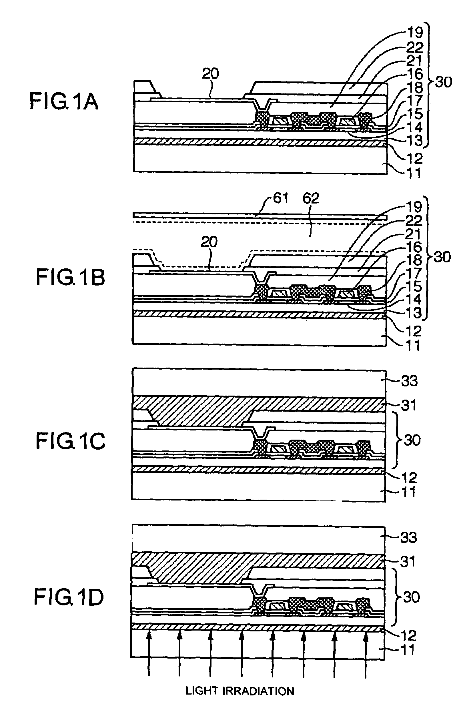
[0031]An exemplary embodiment of the present invention is described below with reference to the drawings. According to the exemplary embodiment of the present invention, a functional element, such as a fine structure, a thin-film circuit, etc., is formed on a first substrate made of quartz glass, alkali glass, etc. The functional element is shifted onto a second substrate by the transfer method described above. In the formation of the functional element on the first substrate, the film-patterning is carried out by photolithography. On the other hand, film-patterning on the second substrate is not carried out by the photography. Film-patterning required after the transferring is carried out by a technique not using mask-alignment, such as a liquid-drop jetting method. Thus, it is desirable to carry out the film-patterning on only the first substrate.

[0032]For example, in the case in which the thin-film device is an organic EL display device, the process from the first step to the ste...

second exemplary embodiment

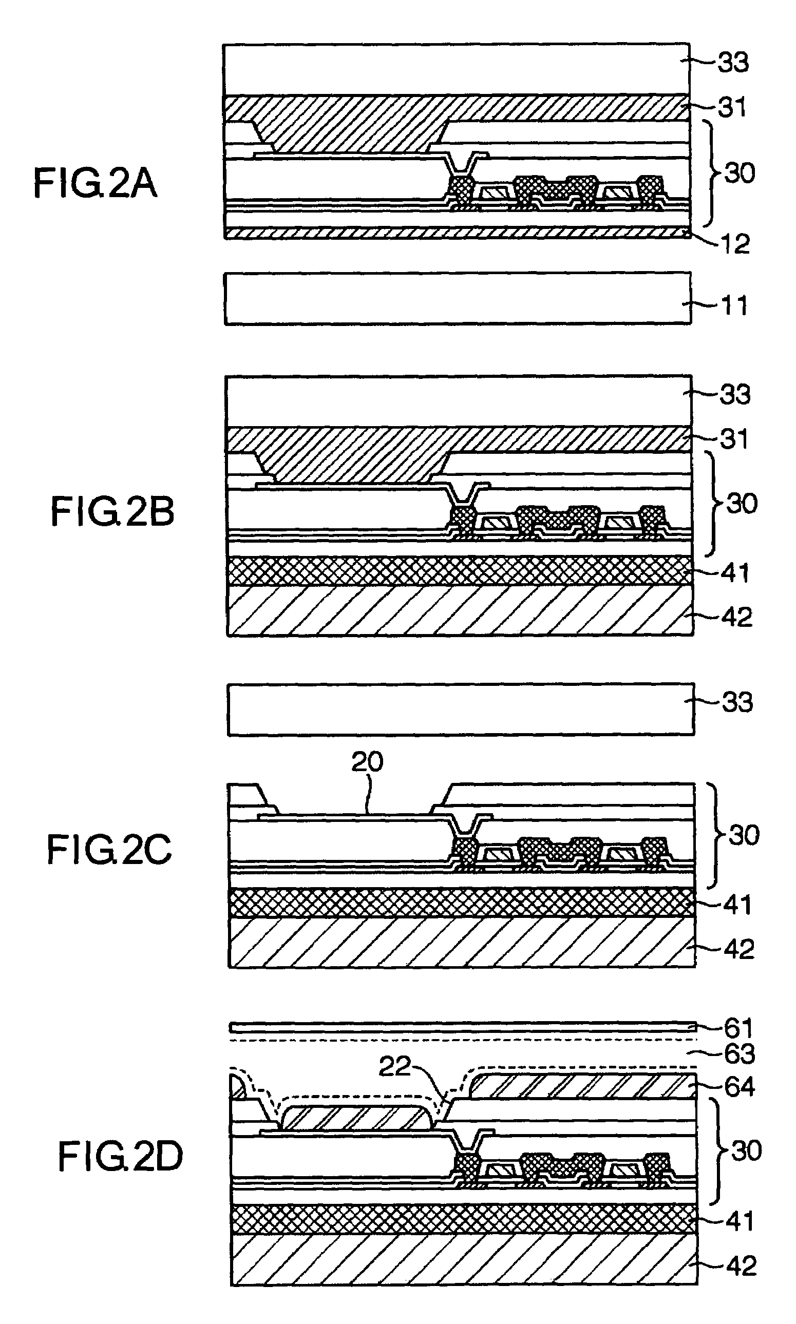
[0052]The second exemplary embodiment is described below with reference to FIGS. 4A to 5D. The elements in these drawings corresponding to those in FIGS. 1A to 1D and FIGS. 2A to 2D are represented by the same reference numerals, and their descriptions are not repeated.

[0053]According to the second exemplary embodiment, the above-described liquid-repelling treatment of the bank layer 22 (FIG. 2D) is not carried out, but the bank layer 22 itself is formed in a film-shape by use of a material having a liquid-repelling property. Thus, the bond of the bank layer 22 to the adhesive layer 31 may become insufficient. Accordingly, an intermediate layer 23 is formed between the bank layer 22 and the adhesive layer 31. A required bonding force between the bank layer 22 and the adhesive layer 31 is secured by the intermediate layer 23. The intermediate layer 23 is removed after the thin-film circuit layer 30 is transferred onto the final substrate. The light-emission area is treated so as to h...

third exemplary embodiment

[0060]The third exemplary embodiment is described below with reference to FIGS. 6A–6E. In FIGS. 6A–6E, elements equivalent to those in FIG. 2C are represented by the same reference numerals. Descriptions of the equivalent elements are not repeated.

[0061]According to the third exemplary embodiment, an organic EL display device is produced by a mask-evaporation method instead of the liquid-drop jetting method used in the first exemplary embodiment. The thin-film circuit layer 30 including a fine structure is formed on the first substrate by photolithography, and is transferred onto the second exemplary embodiment, similarly to the first exemplary embodiment.

[0062]In the case where the organic EL display is produced by the mask-evaporation method, the bank 22 described in the first exemplary embodiment is not necessary. Thus, the thin-film circuit layer 30 formed by the process of the first step to the opening in the pixel area is transferred (FIG. 6A).

[0063]Then, an organic El materia...


PUM

PropertyMeasurementUnit
lengthaaaaaaaaaa
lengthaaaaaaaaaa
electroconductiveaaaaaaaaaa

Abstract

The invention provides a transfer technique by which the dimensional precision of a thin-film device is not deteriorated, even if the device is produced by transferring a fine structure or a thin-film circuit layer onto a substrate with an inferior shape-stability. The method includes: forming a fine structure or a thin-film circuit layer on a first substrate using a photolithographic patterning process; shifting the fine structure or the thin-film circuit layer from the first substrate onto a second substrate, or shifting the fine structure or the thin-film circuit layer from the first substrate onto the second substrate via a third substrate; and forming a thin-film pattern on the fine structure or the thin-film circuit layer shifted onto the second substrate by a non-photolithographic method.

Description

[0001]This application claims priority from Japan Patent Application No. 2003-146165, filed on May 23, 2003, the entire contents of which are hereby incorporated by reference.BACKGROUND OF THE INVENTION[0002]1. Field of Invention[0003]The present invention relates to a method of producing a thin-film device using a transferring technique by which a thin-film circuit layer or a fine structure formed on an element-formation substrate is transferred onto another substrate.[0004]2. Description of Related Art[0005]For related art devices, such as liquid-crystal displays (LCD), organic EL displays, etc., it may be desirable to use a plastic substrate as a base so that the devices are prevented from being broken when they are deformed or dropped, or so that the cost of the devices is reduced.[0006]However, manufacturing thin-film transistors for use in a panel display device, etc., includes a process which is carried out at a relatively high temperature. Thus, problems occur in that plasti...

Claims


Application Information

Patent Timeline
Patent Type & Authority Patents(United States)
IPC IPC(8): H01L21/4763H01L21/44G02F1/1368G02F1/136H01L21/00H01L21/02H01L21/336H01L21/68H01L21/77H01L21/84H01L27/00H01L27/12H01L27/32H01L29/786H01L51/50H01L51/56H05B33/10H05B33/14
CPCH01L21/6835H01L27/1214H01L27/1266H01L29/78603H01L27/3244H01L2924/30105H01L2221/68359H01L2221/68368H01L2251/5338H01L27/1218H10K59/12H10K2102/311F16H57/029B01F27/00B01F35/30B01F2101/305
Inventor UTSUNOMIYA, SUMIO
Owner SAMSUNG ELECTRONICS CO LTD
Why Eureka
Try Eureka