

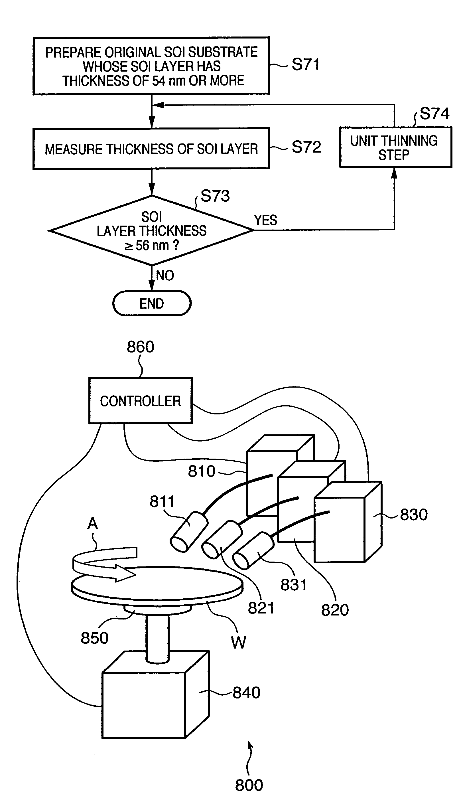
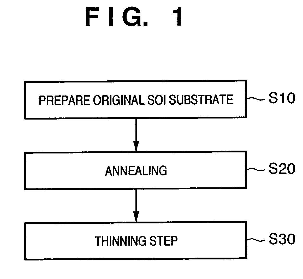
Substrate manufacturing method and substrate processing apparatus
a manufacturing method and substrate technology, applied in semiconductor/solid-state device testing/measurement, bridge structural details, construction, etc., can solve the problems of mechanical damage the thickness of the soi layer is reduced, and the present polishing is difficult to stop, so as to achieve the effect of facilitating the thickness control of the soi layer, eliminating major factors, and high surface planarity
- Summary
- Abstract
- Description
- Claims
- Application Information
AI Technical Summary
Benefits of technology
Problems solved by technology
Method used
Image

Examples
first example
[0137]This example provides a result obtained by comparing a thinning step in units of a predetermined thickness not more than that of one lattice according to the present invention with another method. FIG. 12 is a table comparing the rms values (1 μm□, 2 μm□, 5 μm□, 10 μm□, and 20 μm□) of the surfaces of SOI substrates obtained after thinning, i.e., when a thinning step is performed according to the present invention (“present invention” in FIG. 12), when oxide film etching is performed after thermal oxidation (“after thermal oxidation / oxide film etching” in FIG. 12), and when etching using SC-1 is performed (“after SC-1 etching” in FIG. 12).
[0138]With the thinning step in units of the predetermined thickness not more than that of one lattice according to the present invention, the microroughness of a thin film degrades extremely slightly.
example 2
[0139]This example provides the film thickness distribution of an SOI layer before and after a thinning step in units of a predetermined thickness not more than that of one lattice according to the present invention.
[0140]FIG. 13 shows results obtained by measuring the film thickness distribution of the SOI layer at 17 in-plane points (Position=1 to 17) of an SOI substrate before and after thinning the SOI substrate by 40 nm using the predetermined thickness not more than that of one lattice according to the present invention. With the thinning step according to the present invention, the variation range of the in-plane film thickness of the SOI substrate is kept extremely small even after the thinning.
example 3
[0141]This example provides an application of the present invention to ELTRAN (registered trademark).
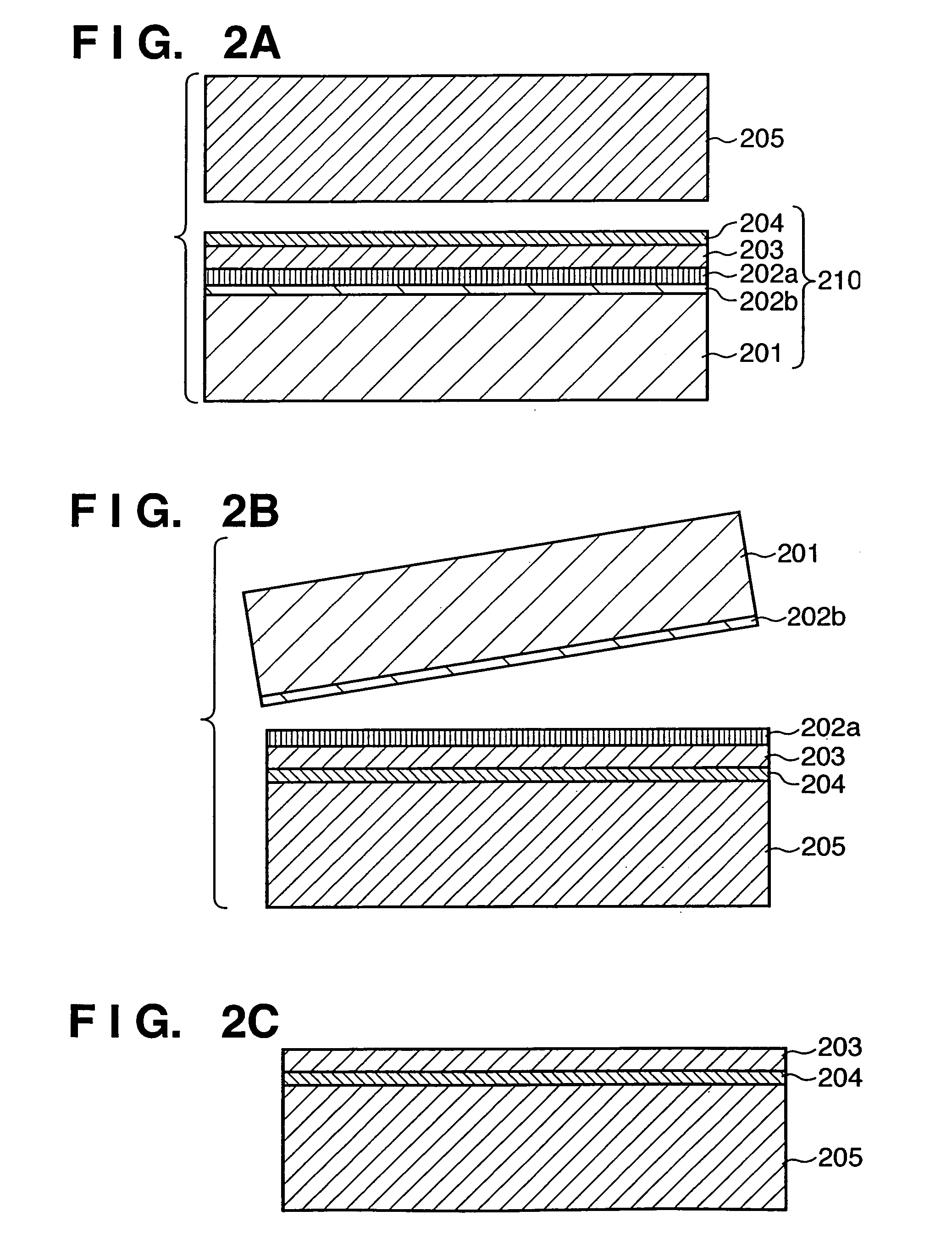
[0142]An original SOI substrate as schematically shown in FIG. 2C was formed using ELTRAN (registered trademark) (S10). The original SOI substrate was so formed as to have an SOI layer 203 with a thickness of 45 nm and a buried oxide film 204 with a thickness of 50 nm. The surface roughness of the original SOI substrate was measured at a 1-μm×1-μm region with an AFM. The resultant rms value was 10.5 nm.
[0143]The original SOI substrate was annealed (planarized) at 1,050° C. for 1 hr in a 100% hydrogen atmosphere (S20). The surface roughness of the SOI layer after the planarization was measured at a 1-μm×1-μm region with the AFM. It was confirmed that the surface roughness improved, i.e., the resultant rms value decreased to 0.09 nm. The film thickness of the SOI layer after the planarization was measured with an ellipsometer and was found to be 44 nm.
[0144]The original SOI substrate a...
PUM
| Property | Measurement | Unit |
|---|---|---|
| thickness | aaaaa | aaaaa |
| thickness | aaaaa | aaaaa |
| thicknesses | aaaaa | aaaaa |
Abstract
Description
Claims
Application Information