Air gap formation

a technology of air gaps and air gaps, which is applied in the direction of instruments, semiconductor/solid-state device details, instruments, etc., can solve the problems of high capacitance loss, large cross-talk, and low-k materials that have not been used in all applications

Active Publication Date: 2007-08-14
SHIPLEY CO LLC
View PDF29 Cites 58 Cited by
  • Summary
  • Abstract
  • Description
  • Claims
  • Application Information

AI Technical Summary

Problems solved by technology

This increase in capacitive coupling causes problems, such as greater cross-talk and higher capacitive losses.
However, low-k materials have not been used in all applications as they can possess severe processing, cost and materials problems.
The air gap forming techniques that have been developed have varying degrees of complexity but typically employ a material disposed between metal lines that is subsequently removed to provide an air gap.
However, these techniques are not without problems.
This method may be detrimental to other layers in the structure, particularly organic low-k dielectric materials used elsewhere in the structure.
Further, photoresists contain a variety of components which make control of the decomposition temperature difficult.
Thus, photoresists may take a long time to be removed entirely and / or require harsh conditions to ensure complete removal of all the photoresist components.
However, such polycycloolefin polymers are expensive to make and may require relatively high decomposition temperatures, e.g. 380 to 450° C. Such temperatures may be detrimental to other materials used in the fabrication of electrical interconnects.
In addition, polycycloolefin polymers are typically prepared using metal catalysts which may contaminate the polymer and result in metal ion contamination in the air gap formed from these polymers.

Method used


Image

  • Air gap formation
  • Air gap formation
  • Air gap formation

Examples


examples 1 – 28

EXAMPLES 1–28

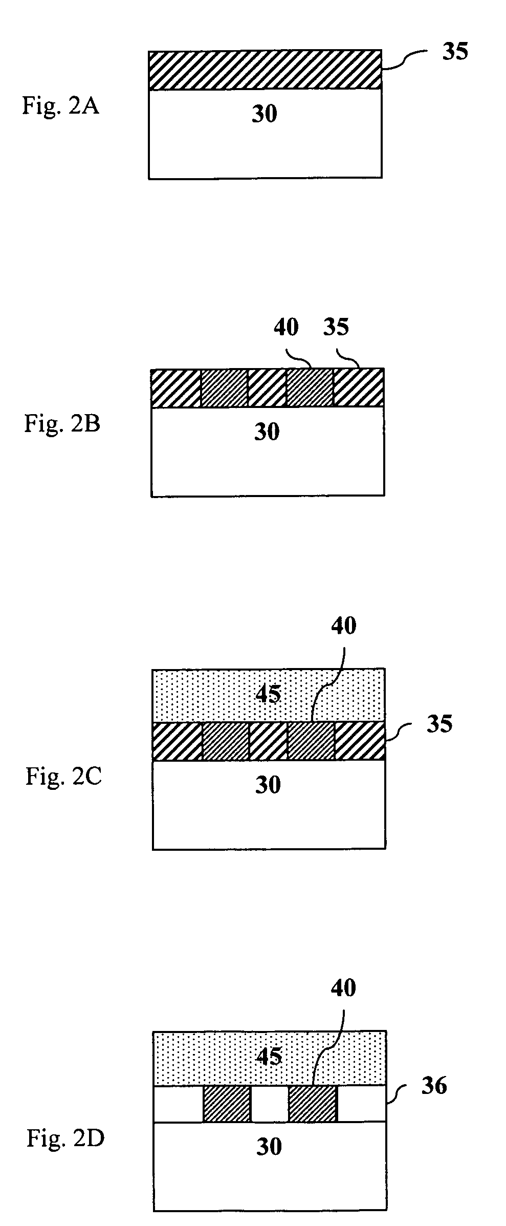
[0080]Cross-linked polymer particles are prepared using the solution polymerization techniques disclosed in U.S. Pat. No. 6,420,441 B1 (Allen et al.). The compositions of the cross-linked polymers are shown in Table 1.

[0081]

TABLE 1ExampleCross-linked Polymer Particle Composition (wt / wt)1MMA / TMPTMA (50 / 50)2TMPTMA (100)3Styrene / TMPTMA (70 / 30)4HEMA / TMPTMA (70 / 30)5HEMA / ALMA (70 / 30)64-Vinyl toluene / TMPTMA (70 / 30)7HPMA / TMPTMA (70 / 30)83-(Trimethoxysilyl) propyl methacrylate / TMPTMA (70 / 30)9Styrene / PETMA (65 / 35)10HEMA / PETMA (75 / 25)11HPMA / ethoxypropyl trimethacrylate (75 / 25)12Styrene / HEMA / ethoxypropyl trimethacrylate (45 / 25 / 30)13MMA / trimethyleneglycol dimethacrylate (70 / 30)14MMA / PETA (75 / 25)15MMA / Styrene / trimethyleneglycol dimethacrylate (30 / 40 / 30)16HPMA / diethyleneglycol dimethacrylate (65 / 35)17HEMA / diethyleneglycol dimethacrylate (60 / 40)18Styrene / HPMA / EGDMA (40 / 20 / 40)19Styrene / ethoxypropyl trimethacrylate (60 / 40)203-(trimethoxysilyl)propyl methacrylate / Styrene / TMPTA (15 / 50 / 35)21...

example 30

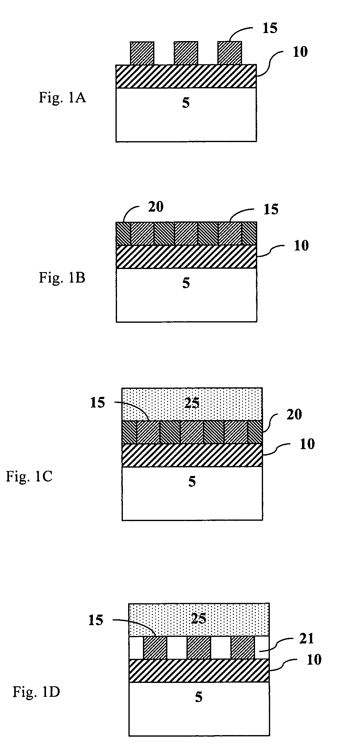
[0082]Compositions are prepared containing cross-linked polymers of any one of Examples 1–29 in a suitable solvent for spin coating, such as propylene glycol monomethyl ether acetate. These compositions are then spin coated on a series of wafers to form a sacrificial material film. The wafer is then soft-baked at 150° C. for 1 minute to remove the solvent. An organic polysilica material containing methylsilsesquioxane and phenylsilsesquioxane and a cross-linked polymer particle as a removable porogen is then disposed on the surface of the sacrificial material as an overlayer material. The organic polysilica is soft-baked at 90° C. for 10 minutes, followed by baking at 130° C. to cure the organic polysilica material. A commercial photoresist is next applied to the organic polysilica. The photoresist is then baked, imaged, and developed. The organic polysilica material and the sacrificial material are then etched to form a pattern and the photoresist is then removed, tantalum / tantalum...

example 31

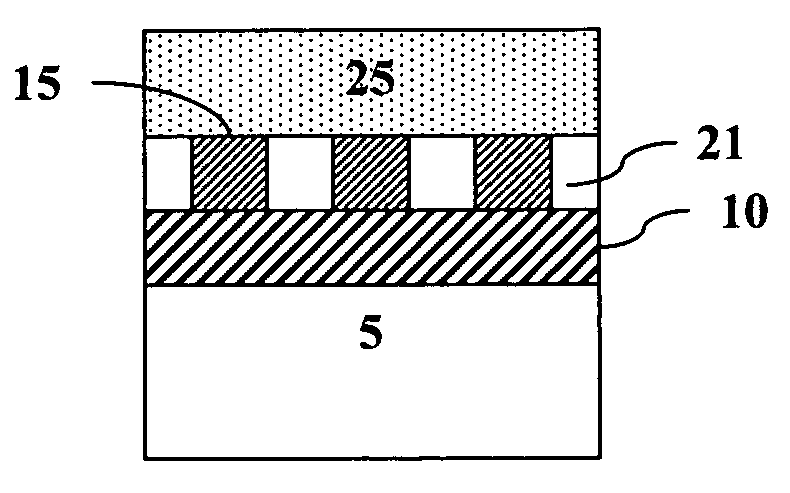
[0083]The procedure of Example 30 is repeated except that the order of steps is changed. After the sacrificial material is disposed on the wafer and dried, it is patterned using conventional lithographic techniques, followed by etching and barrier layer deposition. Copper is next deposited into the etched features on the wafer and the wafer is then planarized. Following planarization, an organic polysilica material containing methylsilsesquioxane and phenylsilsesquioxane and a cross-linked polymer particle as a removable porogen is then disposed on the surfaces of the sacrificial material and the copper lines as an overlayer material. The organic polysilica is soft-baked at 90° C. for 10 minutes, followed by baking at 130° C. to cure the organic polysilica material. The removable porogen in the organic polysilica material is then removed by heating the wafer at 250° for 1 hour to form a porous organic polysilica overlayer material. Next, the wafer is heated at 400–450° C. for 1 hour...


PUM


Abstract

A method of forming air gaps within a solid structure is provided. In this method, a sacrificial material is covered by an overlayer. The sacrificial material is then removed through the overlayer to leave an air gap. Such air gaps are particularly useful as insulation between metal lines in an electronic device such as an electrical interconnect structure. Structures containing air gaps are also provided.

Description

[0001]This Application claims the benefit of Provisional Application Ser. No. 60 / 414,857, filed on Sep. 13, 2002, and Provisional Application Ser. No. 60 / 442,162, filed on Jan. 23, 2003.BACKGROUND OF THE INVENTION[0002]This invention relates generally to the field of electronic device manufacture. In particular, this invention relates to the manufacture of electronic devices using air gaps to reduce capacitive coupling between conductors in such devices.[0003]Advances in integrated circuit technology have reduced the spacing between the metal lines on any given plane of an integrated circuit. Such spacing is now in the sub-micron range. Reducing the spacing between conductive members in the integrated circuit results in an increase in capacitive coupling between nearby conductive traces. This increase in capacitive coupling causes problems, such as greater cross-talk and higher capacitive losses.[0004]Conventional dielectric materials have a dielectric constant in the range of 3.5 t...

Claims


Application Information

Patent Timeline
Patent Type & Authority Patents(United States)
IPC IPC(8): H01L21/311B81B7/00H01L21/764H01L21/768H01L23/522
CPCB81B7/0006H01L21/764H01L23/5222H01L21/7682B81B2203/0315B81C2201/0108Y10T428/24628H01L2924/0002H01L2924/00H01L21/768
Inventor GALLAGHER, MICHAEL K.GRONBECK, DANA A.ADAMS, TIMOTHY G.CALVERT, JEFFREY M.
Owner SHIPLEY CO LLC
Why Eureka
Try Eureka