Sample repairing apparatus, a sample repairing method and a device manufacturing method using the same method

a sample repairing and repair method technology, applied in the direction of mass spectrometers, nuclear engineering, material analysis using wave/particle radiation, etc., can solve the problems of inability to repair opaque defects, inability to accurately detect the damage, etc., to reduce the number of cleaning operations of the optical column, fine-controlled repairing, and the edge roughness of the repaired pattern can be reduced

Inactive Publication Date: 2007-08-14
EBARA CORP
View PDF4 Cites 21 Cited by
  • Summary
  • Abstract
  • Description
  • Claims
  • Application Information

AI Technical Summary

Benefits of technology

[0006]The present invention has been made in the light of the above-pointed problems pertaining to the prior art, and an object thereof is to provide a sample repairing apparatus, a sample repairing method and a device manufacturing method using the same method, which can reduce an edge roughness in a repaired pattern and also can repair a sample by applying an electron beam-assisted etching or an electron beam-assisted deposition.
[0012]According to the invention as defined In claim 1 or claim 10, the edge roughness in the repaired pattern can be reduced. Further, owing to the objective lens with a structure for the differential exhaust system, an amount of a reactive gas flowing into the electron gun side is reduced, thus reducing the number of cleaning operations of the optical column.

Problems solved by technology

On the other hand, from the reason that the electron beam, if having a higher landing energy, could cause a back scattering after an incidence upon the sample and the reflected beam thereof could emit secondary electrons to contribute to the etching, there is another problem that a precision of processing would be not greater than that limited by the extent of the back scattered electrons.
The repairing apparatus employing the focused ion beam has a problem that an ion implantation to a mask substrate or a damage from an irradiation beam could deteriorate a transmittance in a silica substrate, substantially inhibiting the repair of opaque defect from being carried out, which is considered to be a serious problem especially in the F2 lithography.

Method used


Image

  • Sample repairing apparatus, a sample repairing method and a device manufacturing method using the same method
  • Sample repairing apparatus, a sample repairing method and a device manufacturing method using the same method
  • Sample repairing apparatus, a sample repairing method and a device manufacturing method using the same method

Examples


Embodiment Construction

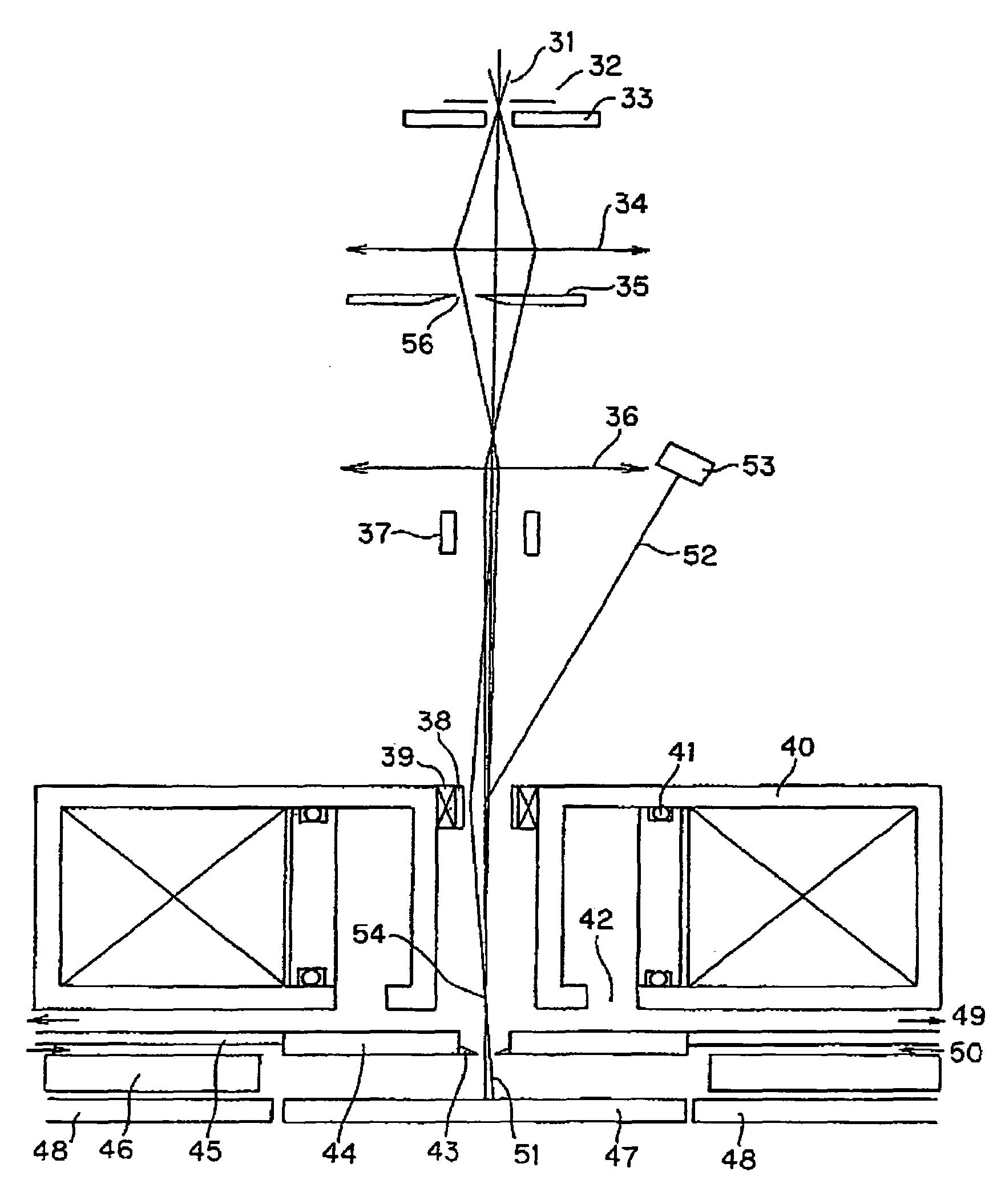
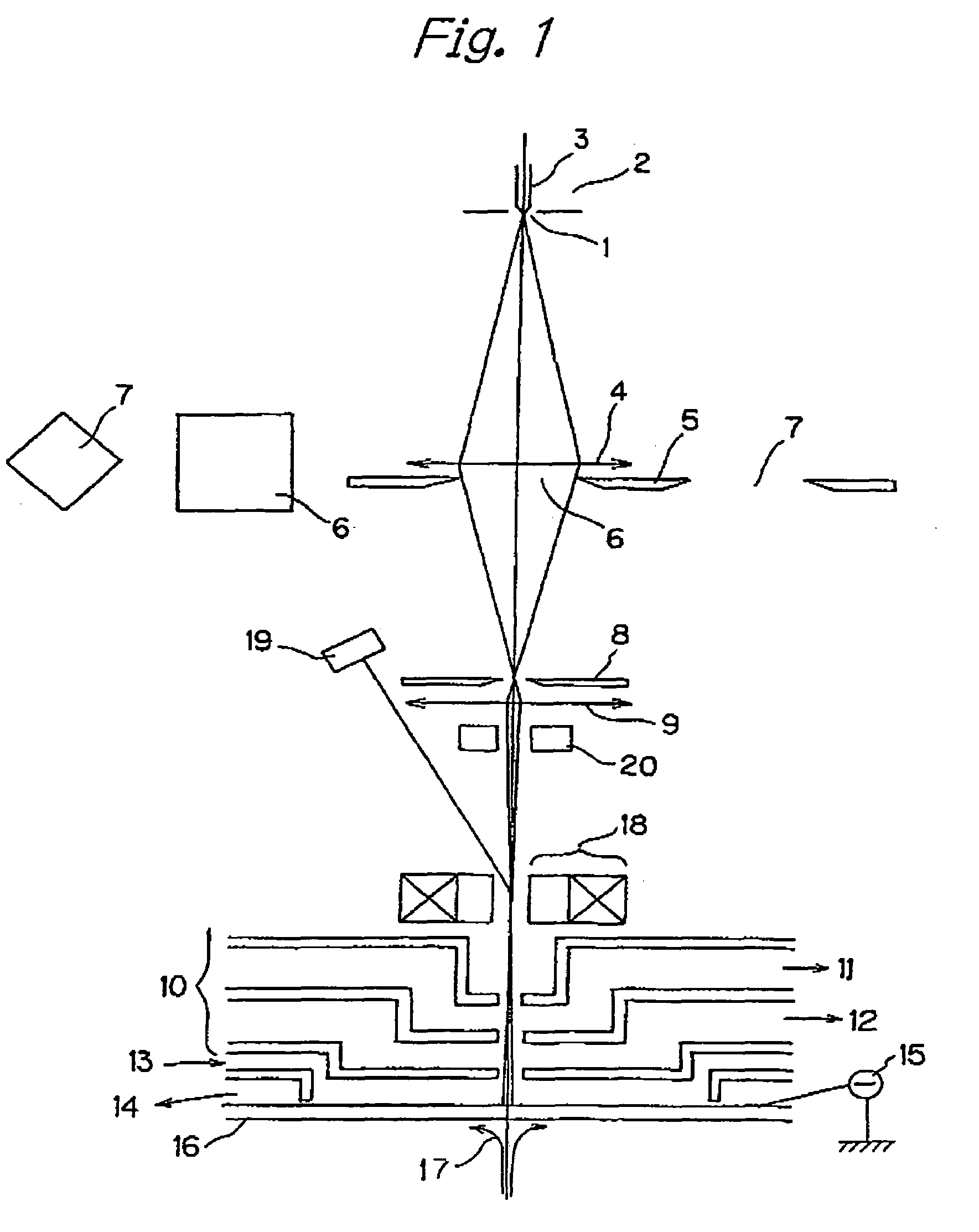
[0071]A best mode for carrying out a sample repairing apparatus, a sample repairing method and a device manufacturing method using the same method according to the present invention will now be described with reference to the attached drawings. FIG. 1 shows schematically an electron beam apparatus (i.e., an electron beam optical column) used in a repairing method of a sample, such as a mask and the like, according to the present invention. As illustrated, an electron gun comprises a Zr-W tip 1, a Schottky shield 2 and a tip heating W filament 3, taking advantage of Schottky emission. An electron beam emitted from this electron gun is focused with a condenser lens 4 to form a crossover image in an NA aperture 8.

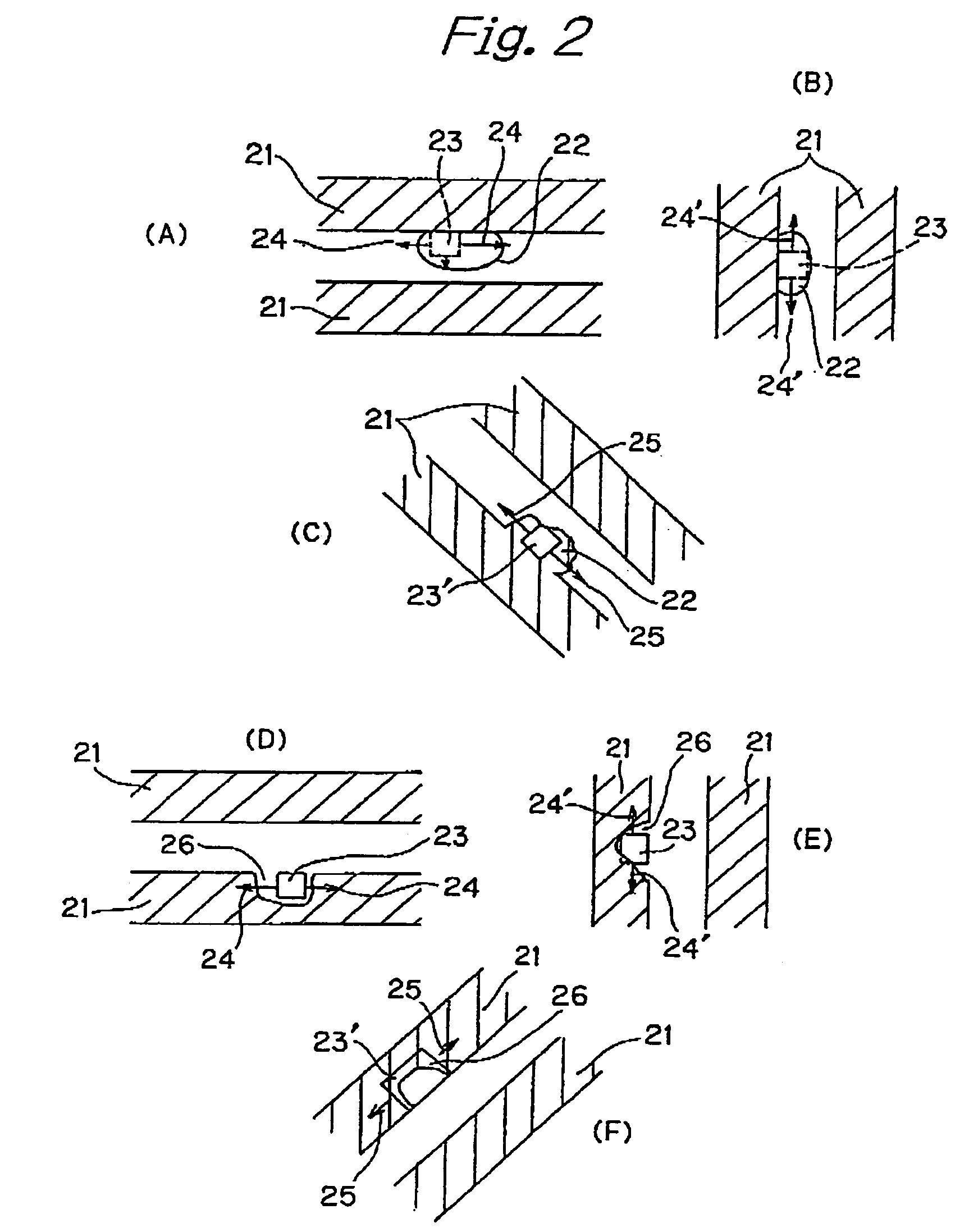
[0072]A shaping aperture plate 5 serving as a shaping aperture Is disposed in a sample (mask) side of a condenser lens 4. The shaping aperture plate 5 includes a rectangular aperture (a first shaping aperture) having sides extending in parallel in the x-direction and the y-dir...


PUM

PropertyMeasurementUnit
landing energyaaaaaaaaaa
widthaaaaaaaaaa
roughnessaaaaaaaaaa

Abstract

An object of the present invention is to provide a sample repairing apparatus, a sample repairing method and a device manufacturing method using the same method, which can reduce an edge roughness in a repaired pattern and also can provide the repairing of a sample by applying an electron beam-assisted etching or an electron beam-assisted deposition. There is provided a sample repairing method comprising: (a) a step of focusing an electron beam by an objective lens to irradiate a sample: (b) a step of supplying a reactive gas onto an electron beam irradiated surface of said sample: (c) a step of selectively scanning a pattern to be repaired on said sample with the electron beam so as to repair said pattern by applying an etching or a deposition; and (d) a step of providing a continuous exhausting operation by means of a differential exhaust system arranged in said objective lens so as to prevent the reactive gas supplied onto said electron beam irradiated surface from flowing toward an electron gun side.

Description

BACKGROUND OF THE INVENTION[0001]The present invention relates to a sample repairing apparatus and a sample repairing method for repairing a defect with high accuracy in a sample, such as a mask, used in the production of a device or the like having a line width equal to or less than 0.1 μm, and further to a device manufacturing method using such a sample repairing method.[0002]There has been a known method in the prior art, in which a sample, such as a mask, is irradiated with a finely focused electron beam and then a reactive gas is blown to the irradiated region thereof with a nozzle so as to carry out the etching of the sample.[0003]When the mask subject to the repairing has the minimum line width as narrow as about 90 nm, the edge roughness in the repaired pattern should be controlled to be of the order of some ten nm or less, which in turn requires to focus the beam to be half a size of the required roughness or smaller than that. On the other hand, from the reason that the el...

Claims


Application Information

Patent Timeline
Patent Type & Authority Patents(United States)
IPC IPC(8): H01J37/30G21K5/10G03F1/00G03F7/20B23K15/00G03F1/72G03F1/74G21K7/00H01J37/08H01J37/18H01J37/305H01J37/317H01L21/027
CPCH01J37/18H01J2237/188H01J2237/31744
Inventor NAKASUJI, MAMORUKATO, TAKAOSATAKE, TOHRUTERAO, KENJIMURAKAMI, TAKESHINOJI, NOBUHARU
Owner EBARA CORP
Why Eureka
Try Eureka