Hermetically sealing a package to include a barrier metal

a technology of barrier metal and hermetically sealing, which is applied in the direction of solid-state devices, generators/motors, basic electric elements, etc., can solve the problems of high cost of forming a small package, vibration portion damage, and inability to reduce the size and height of the baw filter and the saw filter, and achieve reliable bonding and sealing properties. , the effect of high accuracy

Active Publication Date: 2007-08-21
MURATA MFG CO LTD
View PDF7 Cites 44 Cited by
  • Summary
  • Abstract
  • Description
  • Claims
  • Application Information

AI Technical Summary

Benefits of technology

[0032]To overcome the problems described above, preferred embodiments of the present invention provide a method of manufacturing an electr...

Problems solved by technology

However, according to the structure described above, although the size of the elements for the BAW filter and the SAW filter are reduced, when the size of the package is not reduced, the sizes and heights of the BAW filter and the SAW filter cannot be reduced.
In addition, that cost of forming a small package is high.
Furthermore, in particular for the BAW filter, since the vibration portion is provided in an opening or in a concave portion of the substrate, the vibration portion is damaged by impact generated in a step in which an element is processed by dicing, is picked up for mounting, or is die-bonded.
According to Japanese Unexamined Patent Application Publication Nos. 4-293310 and 2000-77970, the following problems may arise since the solder sealing frame is formed at the bond substrate side, and a printing method is used therefor.
Since the solder sealing frame is formed on the bond substrate which is a portion of a mother substrate including a plurality of the bond substrates, when solder is printed on the substrate, cumulative pitch accuracy of the electrodes formed on the mother substrate and the accuracy of a metal mask for printing must be consistent with each other, and as a result, it becomes difficult to form a finer sealing frame.
In addition, since a printing amount of solder that is generated in printing varies due to warping of the mother substrate and variation in electrode thickness, the height of the bumps varies after reflowing, and as a result, bonding defects occur.
Furthermore, in reflowing, since the solder aggregates at corner portions to form convex shapes, the height of the solder varies, and as a result, bonding defects occur.
However, in the method described above, the accuracy of the solder sealing frame cannot be effectively obtained, performance is degraded due to damage to electrodes on the surface of the wafer caused by a printing mask, the wafer is broken by a squeegee printing pressure applied in printing or by heat applied for reflowing the solder, and other defects are likely to occur.
However, since gold having a melting point higher than that of solder is used for the bumps and the sealing frame, the temperature is sig...

Method used


Image

  • Hermetically sealing a package to include a barrier metal
  • Hermetically sealing a package to include a barrier metal
  • Hermetically sealing a package to include a barrier metal

Examples


first preferred embodiment

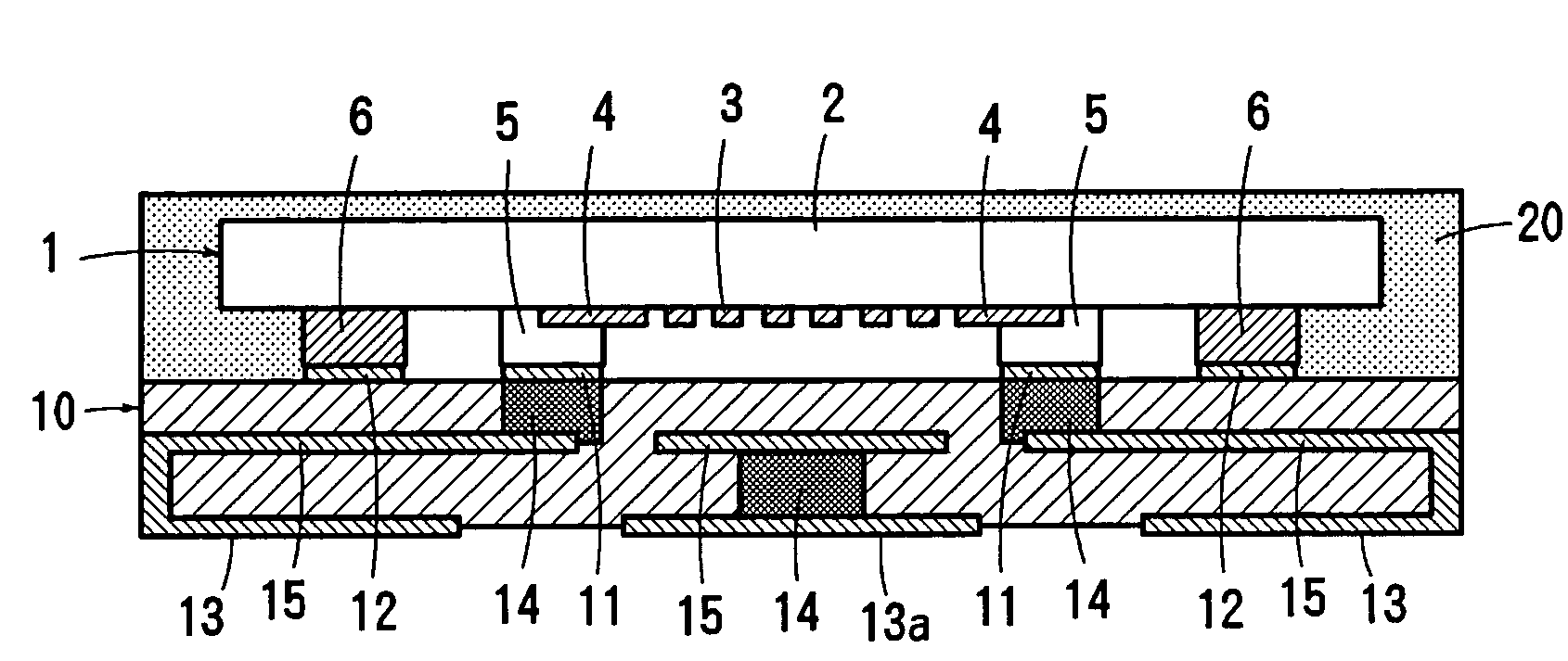
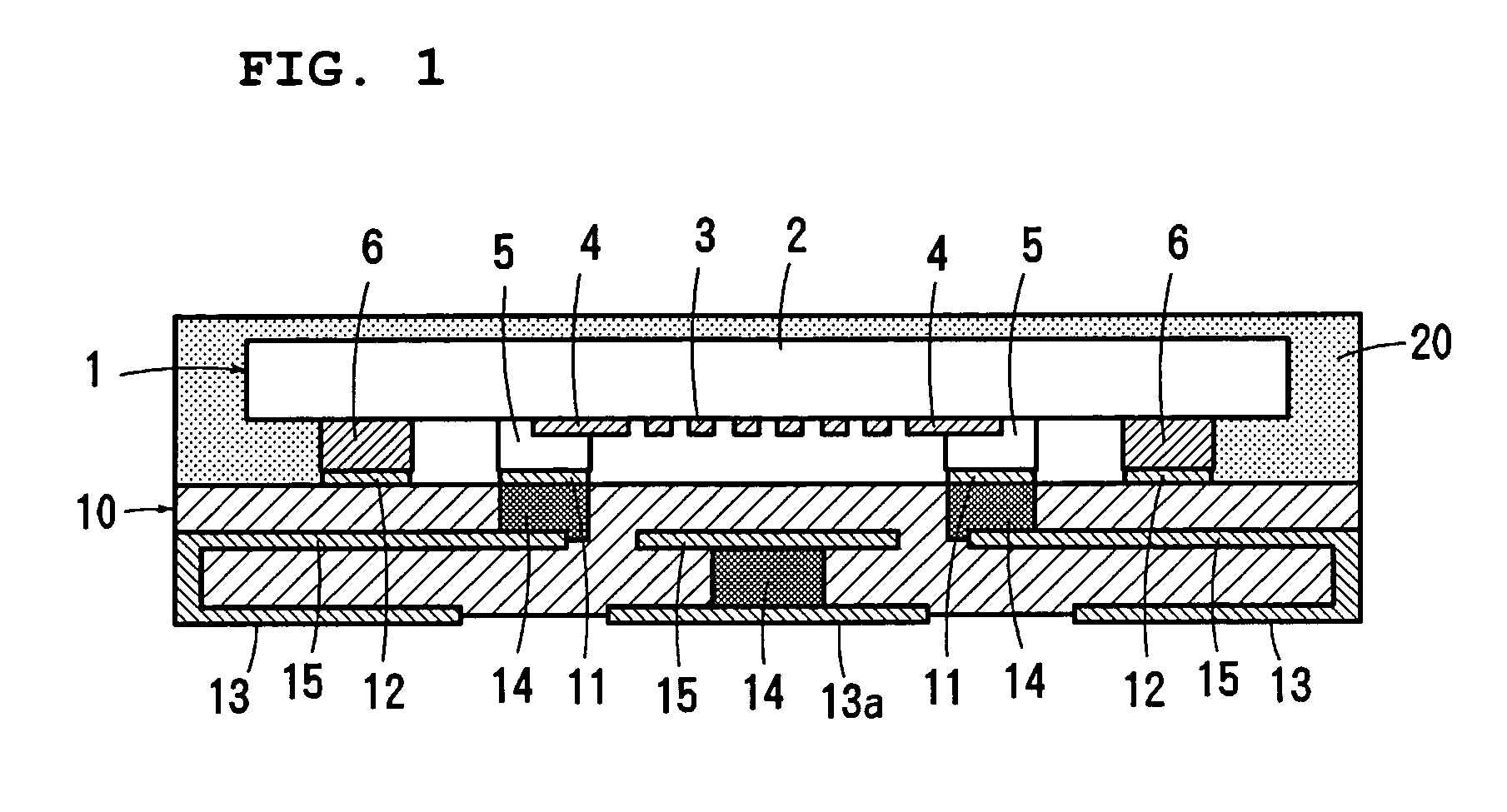
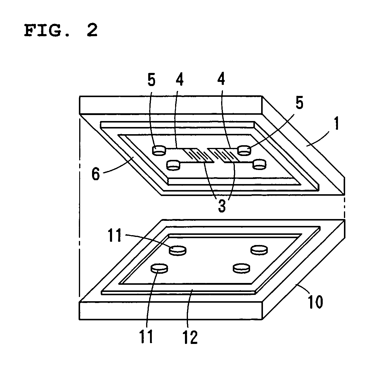
[0074]FIGS. 1 and 2 each show a surface acoustic wave device according to a first preferred embodiment of an electronic device of the present invention. The surface acoustic wave device includes a surface acoustic wave element (hereinafter referred to as a “SAW element”) 1, a bond substrate 10, and a resin 20 coating the periphery of the SAW element 1.

[0075]The SAW element 1 includes a substrate 2 made, for example, of quartz, LiTaO3, LiNbO3, or LiB4O7, having piezoelectric properties, and on one primary surface of the substrate 2, comb-shaped IDT electrodes 3 are provided, terminal electrodes 4 for electrical conduction around the peripheries thereof, solder bumps 5, portions or the entireties of which are provided on the terminal electrodes 4, and a solder sealing frame 6 arranged so as to surround the bumps 5 and IDT electrodes 3. In this example, the width and the thickness of the solder sealing frame 6 are about 70 μm and about 20 μm, respectively, and the diameter and the thic...

second preferred embodiment

[0108]Next, as an electronic device, a BAW filter according to another preferred embodiment of the present invention will be described.

[0109]The basic structure of a piezoelectric thin film resonator is shown in FIGS. 7A and 7B. As shown in FIG. 7A, an opening 61 is provided in an Si substrate 60, and after an insulating film (composed, for example, of SiO2) 62 is provided over the opening 61, a bottom electrode 63, a piezoelectric thin film 64, and a top electrode 65 are formed on the insulating layer 62 in that order. In addition, as shown in FIG. 7B, a concave portion 66 is provided in the Si substrate 60, and after two insulating layers (composed, for example, of SiO2 and Al2O3) 67 and 68 are provided over the concave portion 66, the bottom electrode 63, the piezoelectric thin film 64, and the top electrode 65 are preferably formed on the insulating layer in that order. The electrodes 63 and 65 are preferably formed using Al, Ta, Nb, Mo, Pt, or W, and the piezoelectric thin film...


PUM


Abstract

A method for manufacturing an electronic device includes the steps of forming a first resist pattern on a primary surface of a SAW element, the first resist pattern having openings at positions corresponding to those at which bumps and a sealing frame are to be formed, sequentially forming metals over the first resist pattern, the metals being formed into adhesion layers, barrier metal layers, and solder layers, removing the first resist pattern on the SAW element such that the bumps and the sealing frame are simultaneously formed. When the bumps and the sealing frame of the SAW element are bonded to bond electrodes of the bond substrate, the solder layers are melted and alloyed by heating.

Description

BACKGROUND OF THE INVENTION[0001]1. Field of the Invention[0002]The present invention relates to methods of manufacturing electronic devices, and more particularly, to a method of manufacturing an electronic device in which a communication element, such as a surface acoustic wave filter, a piezoelectric filter using piezoelectric thin-film resonators, an optical signal modulator, or a high-frequency element, is flip-chip mounted on a bond substrate and is then hermetically sealed.[0003]2. Description of the Related Art[0004]In recent years, in accordance with the trend to make electronic apparatuses compact and light weight, multifunctionality has been required for electronic devices. According to the trend described above, piezoelectric devices used for communication apparatuses including mobile phones, such as a surface acoustic wave filter (hereinafter referred to as a “SAW filter”) and a piezoelectric filter (hereinafter referred to as a Bulk Acoustic Wave Filter or “BAW filter”...

Claims


Application Information

Patent Timeline
IPC IPC(8): H01L21/00H01L41/053H01L21/60H03H3/02H03H3/08H03H9/05H03H9/25H03H9/56
CPCH01L24/97H03H3/02H03H3/08H03H9/0557H03H9/059H03H9/1085H03H9/564H01L2221/68345H01L2224/16H01L2224/97H01L2924/01002H01L2924/01004H01L2924/01013H01L2924/01027H01L2924/01029H01L2924/0103H01L2924/01032H01L2924/01042H01L2924/01046H01L2924/01047H01L2924/01049H01L2924/01051H01L2924/01073H01L2924/01074H01L2924/01075H01L2924/01078H01L2924/01079H01L2924/01082H01L2924/01322H01L2924/01327H01L2924/09701H01L2924/163H01L2924/3025H01L2224/85H01L2924/01005H01L2924/01006H01L2924/01024H01L2924/01033H01L2924/01041H01L2924/15787H01L2224/05568H01L2924/00014H01L2924/00H01L2224/05599
Inventor MURATA, KOJIIWAMOTO, TAKASHIHORIGUCHI, HIROKIKUBO, RYUICHIFUJII, HIDETOSHIAIZAWA, NAOKO
Owner MURATA MFG CO LTD
Why Eureka
Try Eureka