
Methods of forming doped and un-doped strained semiconductor materials and semiconductor films by gas-cluster-ion-beam irradiation and materials and film products

a technology of gas-cluster ion beam and semiconductor materials, which is applied in the direction of semiconductor devices, electrical equipment, electric discharge tubes, etc., can solve the problems of unfavorable silicon unfavorable silicon ion implantation efficiency, and high cost per wafer

Active Publication Date: 2007-08-21
EPION
View PDF9 Cites 130 Cited by
  • Summary
  • Abstract
  • Description
  • Claims
  • Application Information

AI Technical Summary

Benefits of technology

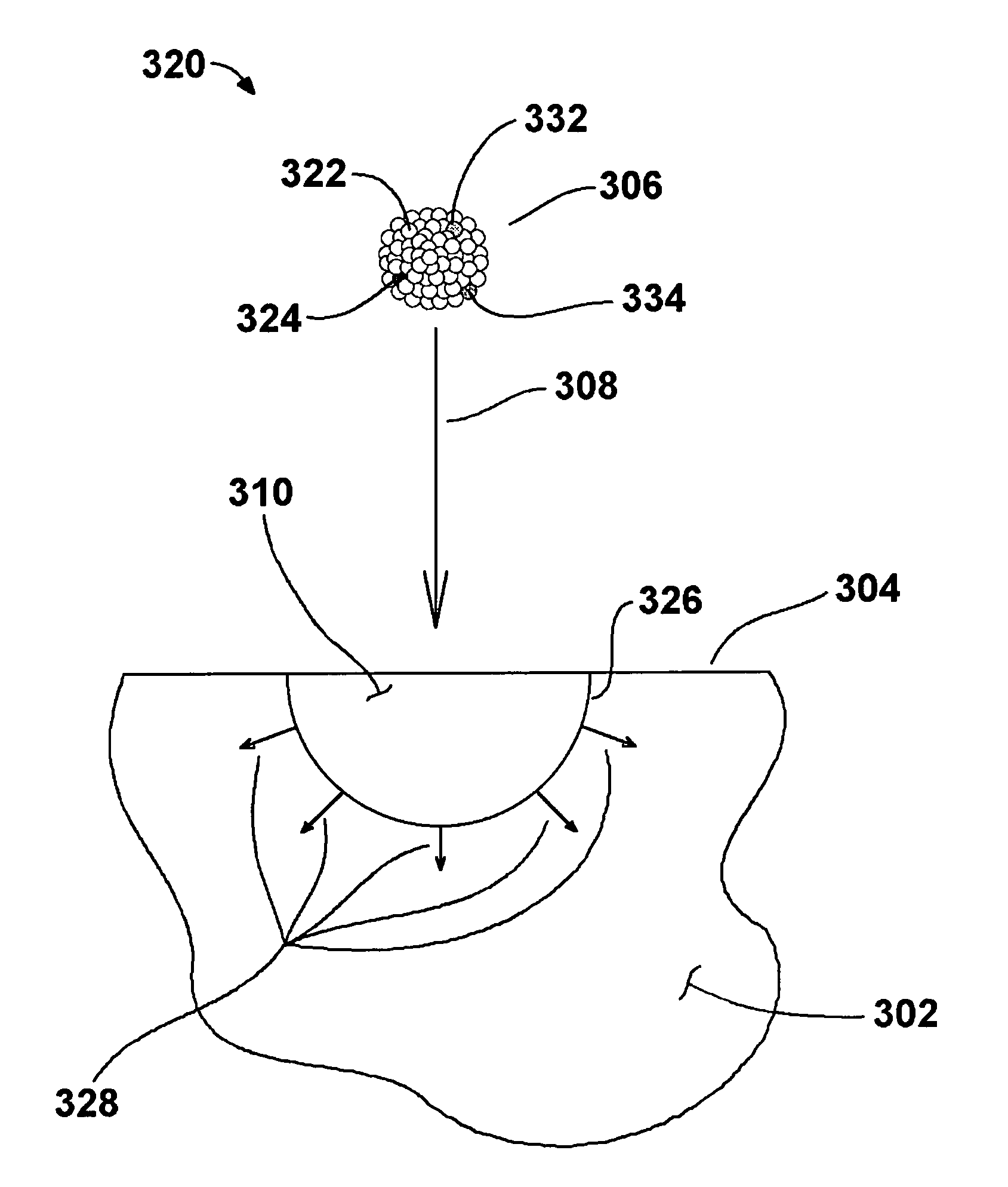
"The present invention provides a method for introducing germanium or other strain-inducing atoms into semiconductor substrates by using energetic cluster ion irradiation. This method can be used to form semiconductor films or strained semiconductor films on the surfaces of semiconductor or dielectric substrates. Additionally, the invention allows for the simultaneous introduction of germanium or other strain-inducing atoms and dopant atoms into semiconductor substrates. The technical effects of this invention include improved semiconductor device performance and the formation of high-quality semiconductor films."

Problems solved by technology

Previous methods (such as epitaxy) for producing blanket strained-silicon on semiconductor or insulating (typically silicon oxide) substrates involve low throughput, high temperature, techniques that result in undesirably high costs per wafer.
Such local-strain techniques have also been expensive to implement and typically utilize high processing temperatures that can be a disadvantage in some applications.
Conventional ion implantation using atomic or molecular ions of materials containing germanium has not proven an efficient way of introducing germanium into silicon for creating strain.
The required high concentrations of at least a few atomic percent of germanium in silicon for effective strain production require such high conventional ion implantation doses so as to be economically impractical with conventional ion implantation equipment.
In general, the solid solubility limit of the dopant in silicon has been an upper limit for effective doping.
Consequently, the impact effects of large clusters are substantial, but are limited to a very shallow surface region.

Method used


Image

  • Methods of forming doped and un-doped strained semiconductor materials and semiconductor films by gas-cluster-ion-beam irradiation and materials and film products
  • Methods of forming doped and un-doped strained semiconductor materials and semiconductor films by gas-cluster-ion-beam irradiation and materials and film products
  • Methods of forming doped and un-doped strained semiconductor materials and semiconductor films by gas-cluster-ion-beam irradiation and materials and film products

Examples


Embodiment Construction

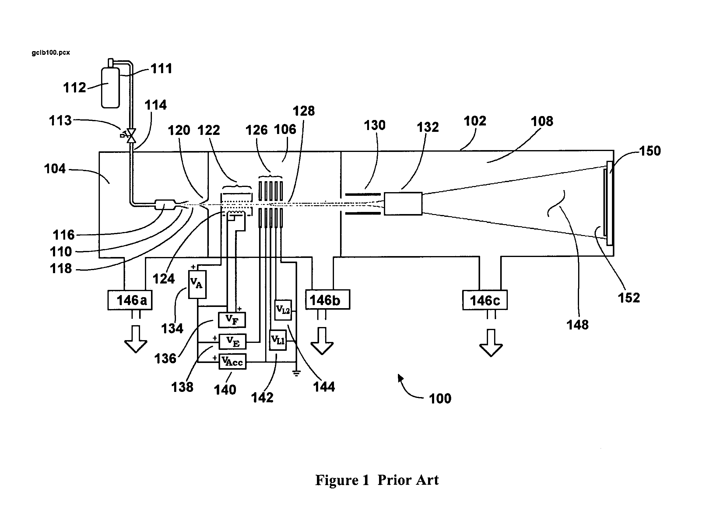
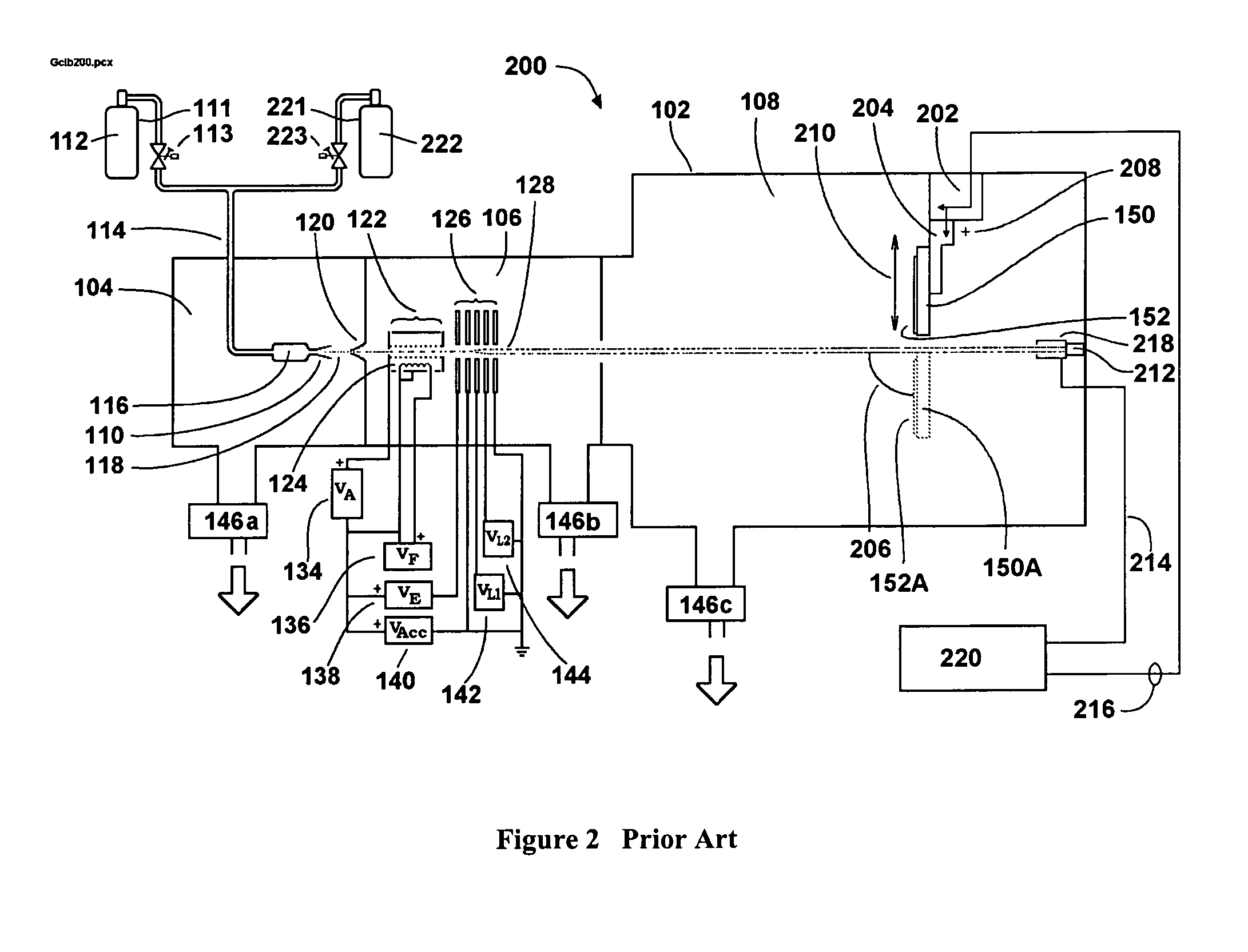
[0031]FIG. 1 shows a schematic of the basic elements of a typical configuration for a processing apparatus 100 for generating a GCIB in accordance with the present invention. Apparatus 100 may be described as follows: a vacuum vessel 102 is divided into three communicating chambers, a source chamber 104, an ionization / acceleration chamber 106, and a processing chamber 108. The three chambers are evacuated to suitable operating pressures by vacuum pumping systems 146a, 146b, and 146c, respectively. A condensable source gas 112 (for example argon or N2) stored in a gas storage cylinder 111 is admitted under pressure through gas metering valve 113 and gas feed tube 114 into stagnation chamber 116 and is ejected into the substantially lower pressure vacuum through a properly shaped nozzle 110. A supersonic gas jet 118 results. Cooling, which results from the expansion in the jet, causes a portion of the gas jet 118 to condense into clusters, each consisting of from several to several th...


PUM

PropertyMeasurementUnit
acceleration voltageaaaaaaaaaa
energyaaaaaaaaaa

Abstract

Methods and apparatus are described for irradiating one or more substrate surfaces with accelerated gas clusters including strain-inducing atoms for blanket and / or localized introduction of such atoms into semiconductor substrates, with additional, optional introduction of dopant atoms and / or C. Processes for forming semiconductor films infused into and / or deposited onto the surfaces of semiconductor and / or dielectric substrates are also described. Such films may be doped and / or strained as well.

Description

CROSS-REFERENCE TO RELATED APPLICATIONS[0001]This application claims the benefit of priority to U.S. Provisional Application Ser. Nos. 60 / 544,516 filed 14 Feb. 2004, and 60 / 621,911 filed 25 Oct. 2004, each entitled “Formation of Doped and Un-Doped Strained Silicon and Semiconductor Films by Gas-Cluster Ion Irradiation”, and both of which are hereby incorporated by reference in their entirety.FIELD OF THE INVENTION[0002]This invention relates generally to the formation of locally strained regions in semiconductor substrates and doped or un-doped thin films of semiconductor materials on semiconductor or other substrates, and more particularly, through energetic gas-cluster ion irradiation.BACKGROUND OF THE INVENTION[0003]The characteristics of semiconductor materials such as, for example, silicon, germanium and gallium arsenide and other semiconductors have been exploited to form a large variety of useful devices in the fields of electronics, communications, electro-optics, and nano-t...

Claims


Application Information

Patent Timeline
Patent Type & Authority Patents(United States)
IPC IPC(8): H01L21/00H01L21/322H01L21/265H01L21/302H01L31/0328
CPCH01L21/265H01L21/26506H01L21/26513H01L21/26566H01L29/7842H01J2237/0812H01L21/2658
Inventor BORLAND, JOHN O.HAUTALA, JOHN J.SKINNER, WESLEY J.TABAT, MARTIN D.
Owner EPION
Learn More