Silicon carbide and other films and method of deposition

a technology applied in the field of silicon carbide and other films, can solve the problems of inability to deposit uniform films of silicon carbide on large-area substrates, development of silicon carbide, and inability to achieve the effect of uniform film formation

Active Publication Date: 2007-08-28
CASE WESTERN RESERVE UNIV
View PDF12 Cites 56 Cited by
  • Summary
  • Abstract
  • Description
  • Claims
  • Application Information

AI Technical Summary

Benefits of technology

[0007]The present invention provides methods of depositing films on a substrate that enables control of the residual stress, residual stress gradient, and electrical resistivity of the deposited film. The invention includes films of various compositions, such as ceramic films with the ceramic compound having a metallic and non-metallic component. Preferably, the film is a silicon carbide film. The silicon carbide film is deposited by chemical vapor deposition onto a substrate, such as a silicon substrate, by placing the substrate in a reaction chamber and evacuating the chamber to a pressure below about 10 mtorr. The temperature of the chamber is maintained at about 900° C. A carbon precursor, such as acetylene (5% in hydrogen) is supplied to the chamber at a flow rate of about 180 standard cubic centimeters per minute (sccm). A silicon precursor, such as dichlorosilane (DCS), is supplied to the chamber at a flow rate of about 54 sccm. As the precursors are supplied, the pressure of the reaction chamber increases and may be maintained at a fixed pressure.

Problems solved by technology

One of the barriers limiting development of silicon carbide in MEMS production has been the inability to deposit uniform films of silicon carbide on large area substrates having properties that are advantageous to and required for MEMS and NEMS.
With single crystalline and polycrystalline silicon carbide, such an approach is not feasible because silicon carbide is chemically and crystallographically stable at conventional annealing temperatures.
For silicon carbide films deposited on silicon substrates, annealing is completely ineffective because the non-silicon carbide substrate limits the annealing temperatures to temperatures too low for effective annealing.

Method used


Image

  • Silicon carbide and other films and method of deposition
  • Silicon carbide and other films and method of deposition
  • Silicon carbide and other films and method of deposition

Examples


example 1

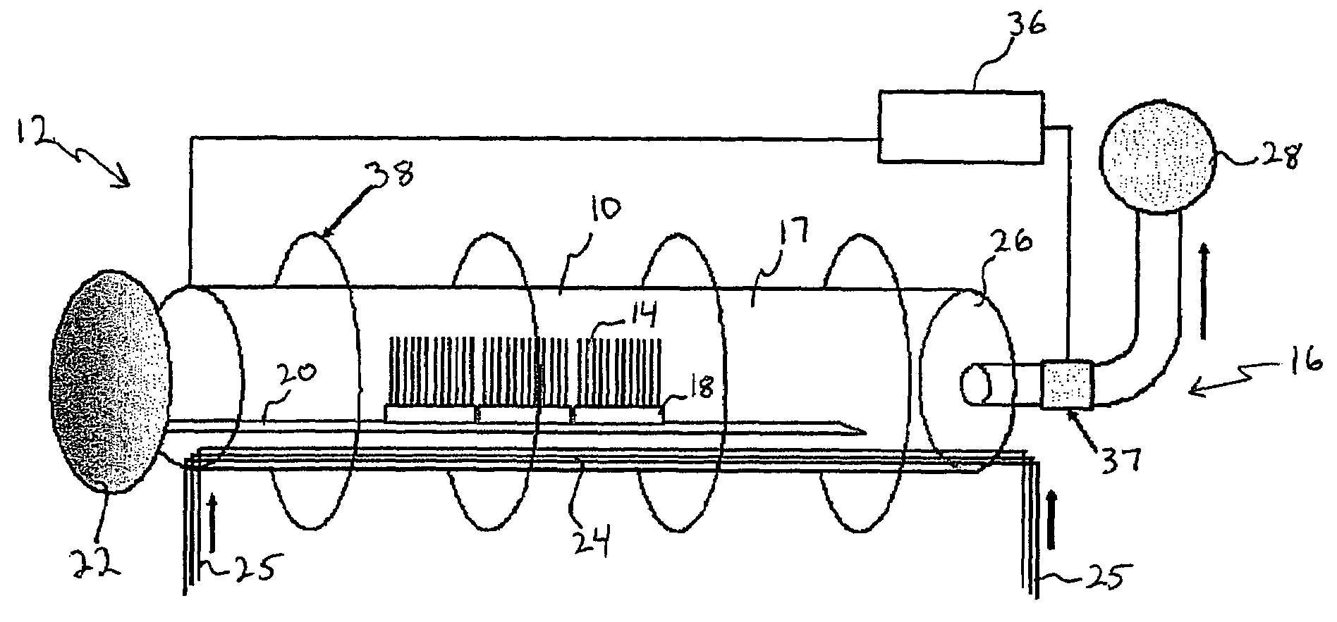
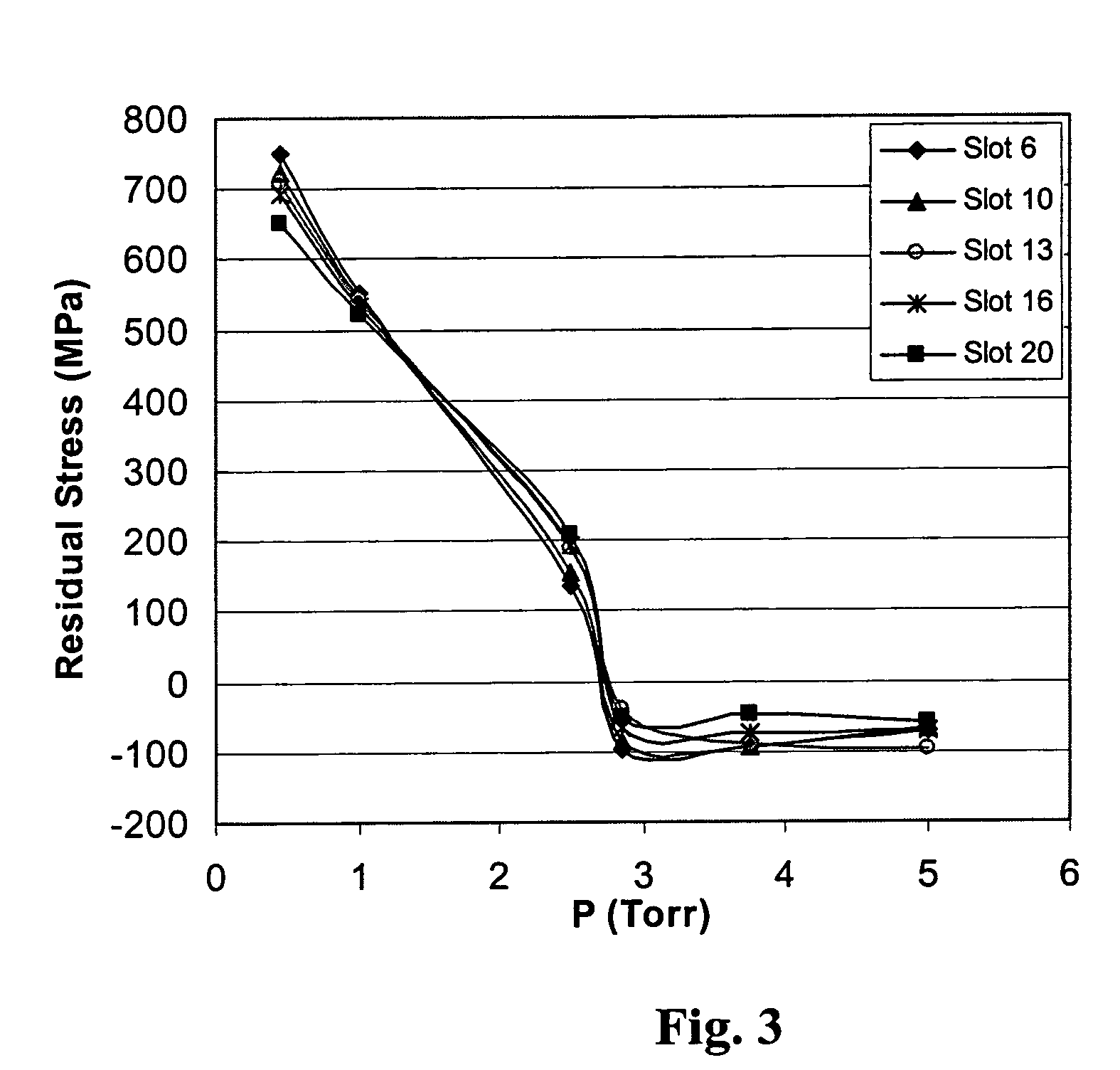
[0038]FIG. 1 illustrates the low pressure chemical vapor deposition apparatus 12 used for these tests. Depositions were performed for two hours at pressure settings from about 0.42 torr to about 5 torr. In several cases, longer times were used to deposit thicker films. The flow rates of DCS and acetylene (5% in hydrogen) were held constant at about 54 standard cubic centimeters per minute (sccm) and 180 sccm, respectively. The temperature was held fixed at about 900° C. The furnace was configured with injector tubes to introduce the acetylene and DCS gases into the reaction chamber.

[0039]Following each deposition, the thickness of the films was measured optically using a Nanospec 4000 AFT spectrophotometer. The film residual stresses were determined by measuring the curvature of the silicon wafers before and after film deposition, using a laser-based curvature measuring system (Frontier Semiconductor measurement, FSM 120). Silicon carbide films were deposited on both sides of the wa...

example 2

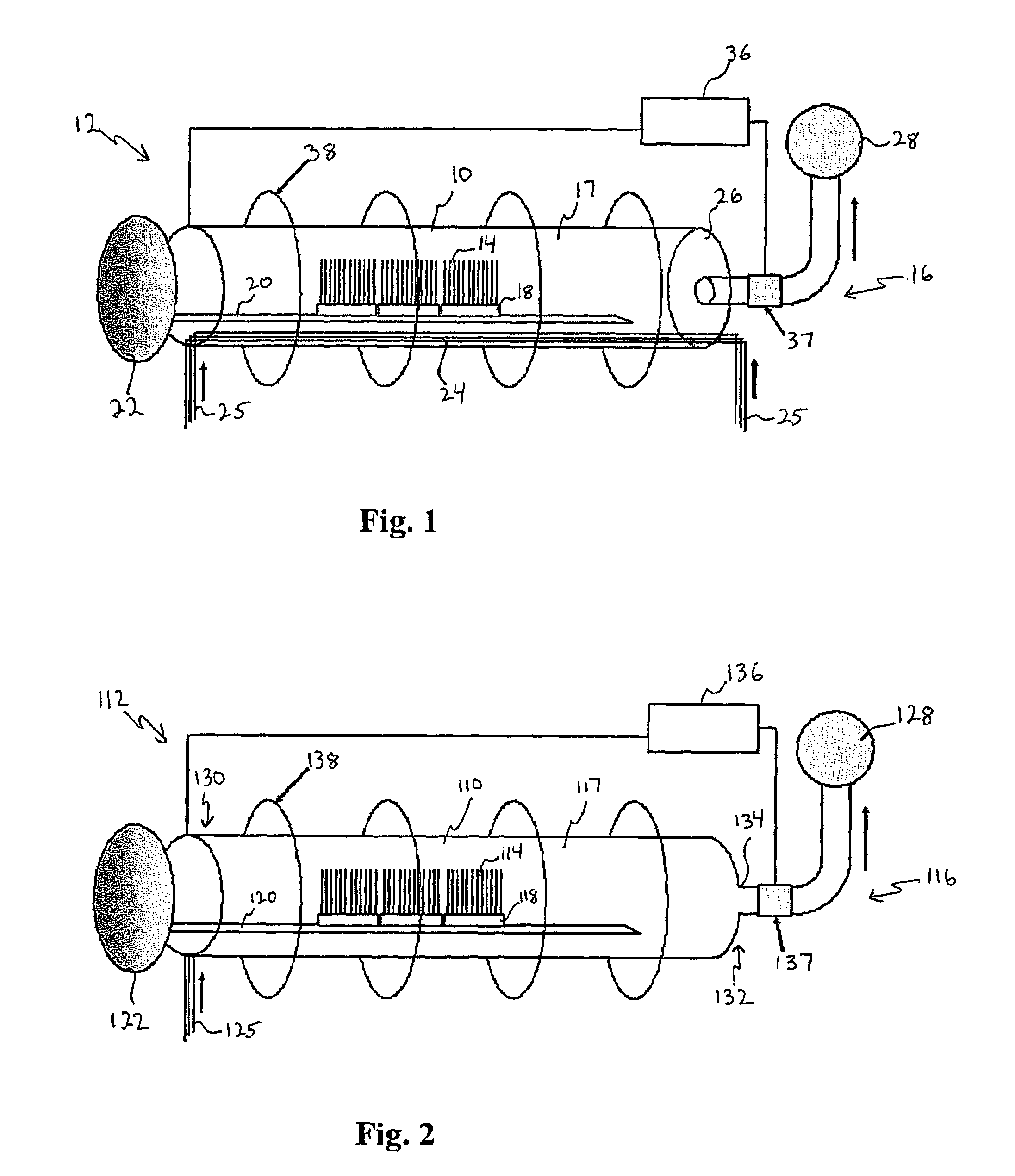
[0044]The same procedure described above was used, except that the low pressure chemical vapor deposition apparatus 112 illustrated in FIG. 2 was used (no injectors, single front flange). For this series of tests, the deposition pressure was maintained essentially constant at about 2.0 torr, and the flow rate of the silicon precursor, in this case DCS, was varied between about 18 sccm and about 54 sccm. The flow rate of acetylene (5% in hydrogen) was fixed at about 180 sccm, and the temperature of the reaction chamber was maintained at about 900° C.

[0045]As above, the films were characterized for residual stress, residual stress gradient, and electrical resistivity. FIG. 6 illustrates the measured residual stress versus the flow rate of the DCS. The observed residual stress decreased as a function of DCS flow rate until a flow rate of 36 sccm. The residual stress was substantially the same at a flow rate of 54 sccm as it was at a flow rate of 36 sccm. The residual stress as a functi...


PUM

PropertyMeasurementUnit
electrical resistivityaaaaaaaaaa
pressureaaaaaaaaaa
pressureaaaaaaaaaa

Abstract

A method of depositing a ceramic film, particularly a silicon carbide film, on a substrate is disclosed in which the residual stress, residual stress gradient, and resistivity are controlled. Also disclosed are substrates having a deposited film with these controlled properties and devices, particularly MEMS and NEMS devices, having substrates with films having these properties.

Description

STATEMENT REGARDING FEDERALLY SPONSORED RESEARCH OR DEVELOPMENT[0001]A part of this invention was made with government support under Contracts No. NCA3-201 awarded by NASA and DABT 63-1-0010 awarded by DARPA. The government has certain rights in this invention.BACKGROUND[0002]The present invention relates to silicon carbide and other films, and, more particularly, to controlled deposition of these films on a substrate.[0003]Semiconductor, micro- and nanoelectromechanical systems (MEMS / NEMS) apply integrated circuit fabrication technology to fabricate optical, mechanical, electrochemical, and biosensor devices. One of the important steps in creating MEMS and NEMS devices is the deposition of thin films of material onto substrates. Once the films are deposited, various etching techniques may be employed to shape the deposited film.[0004]In typical MEMS / NEMS devices, silicon is a primary material. Silicon carbide is a material that has very good physical and chemical characteristics, a...

Claims


Application Information

Patent Timeline
Patent Type & Authority Patents(United States)
IPC IPC(8): C23C16/00B81B3/00C23C16/32C23C16/52G02B26/08H01L21/04
CPCC23C16/325H01L21/20B82Y40/00
Inventor MEHREGANY, MEHRANZORMAN, CHRISTIAN A.FU, XIAO-ANDUNNING, JEREMY L.
Owner CASE WESTERN RESERVE UNIV
Why Eureka
Try Eureka