Check patentability & draft patents in minutes with Patsnap Eureka AI!

Memory circuit comprising an error correcting code

a memory circuit and error correction technology, applied in the field of memory circuits, can solve the problems of penalizing the system's operating speed, memory circuits functioning at high speed are not adapted to use error correction codes, and the load capacity is increasingly low, so as to achieve high operating frequency, high performance, and adapt to high speed

Active Publication Date: 2007-09-18
STMICROELECTRONICS SRL
View PDF3 Cites 9 Cited by
  • Summary
  • Abstract
  • Description
  • Claims
  • Application Information

AI Technical Summary

Benefits of technology

[0012]A main advantage of the present invention is in realizing a memory circuit architecture that is particularly adapted to high speeds while allowing the integration of an error correcting code system.
[0013]A first aspect of the present invention provides a memory architecture adapted to use an error correcting code allowing high operating frequency.
[0014]Another aspect of this invention provides a high performance memory circuit equipped with an error correcting system.
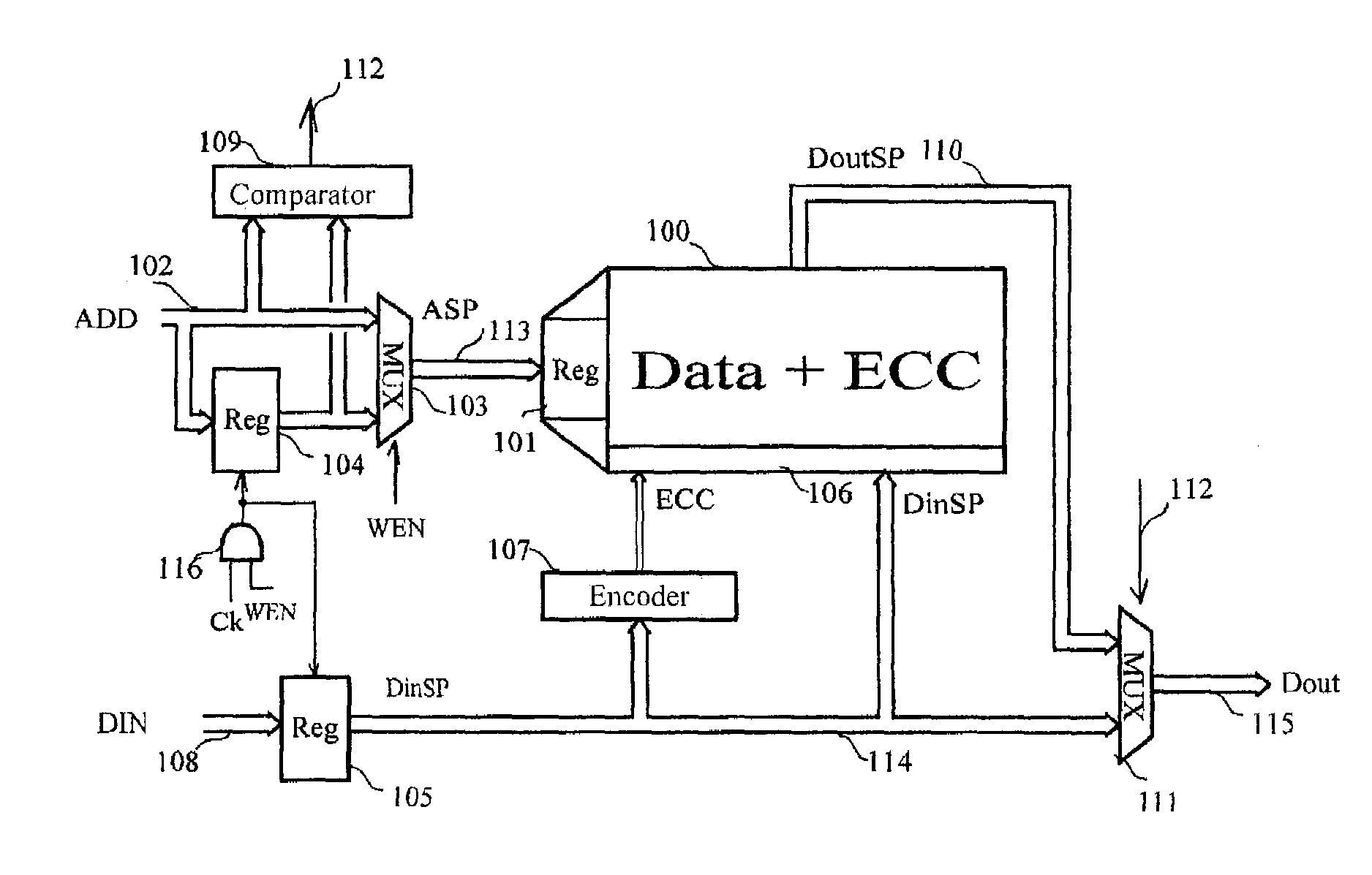
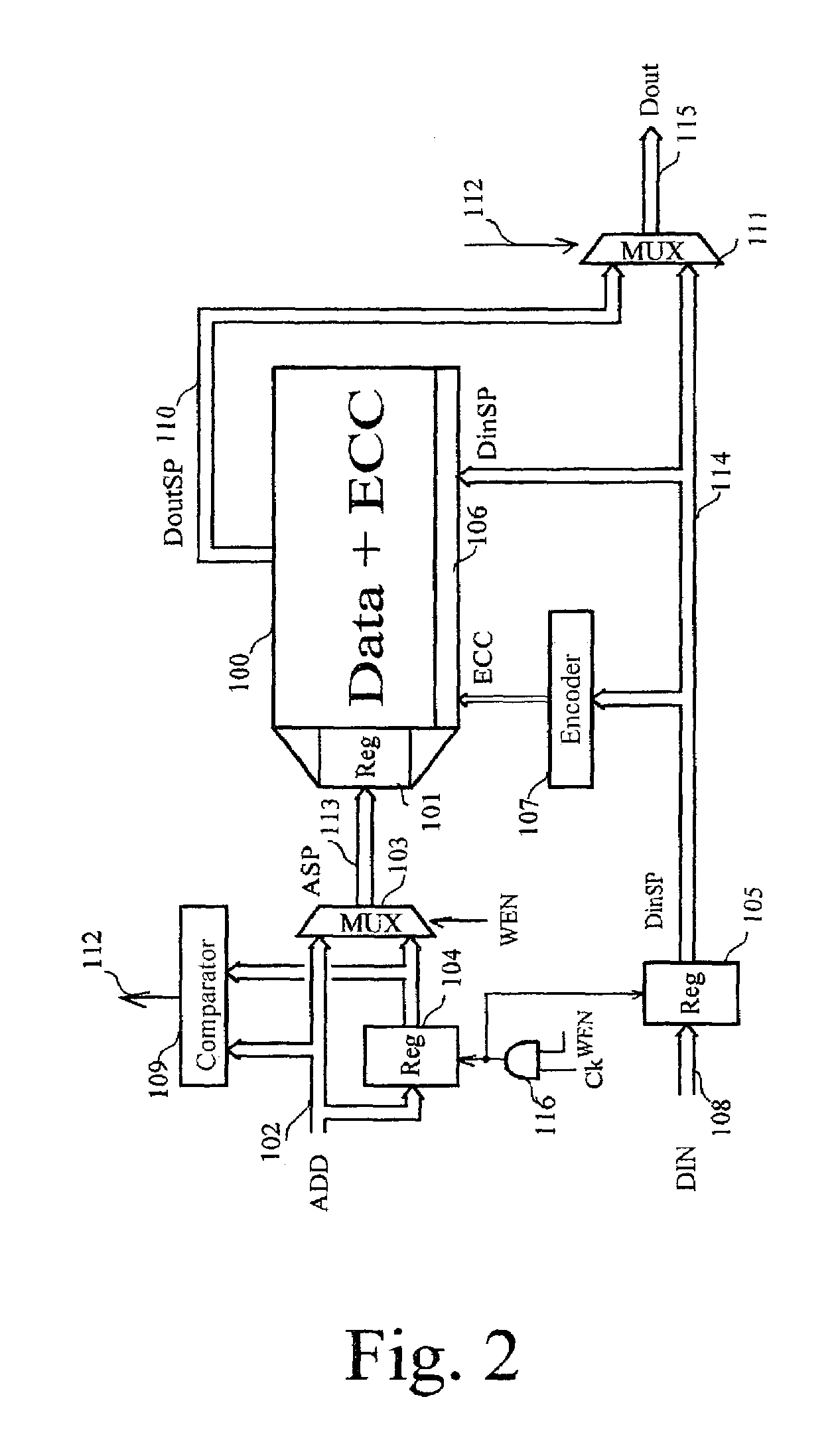
[0015]A preferred embodiment of the invention provides advantages by means of a memory circuit equipped with an error correcting system comprising an address bus, an input data bus, and an output data bus. The circuit comprises a memory that includes its own address bus, its own input data bus and own output data bus, and an error correcting circuit comprising an ECC encoder. The circuit comprises an address shift unit (or address pipeline stage) making it possible to shift write operations in a given cycle to the next write cycle. Read operations remain unchanged.
[0016]As a result the encoder has enough time to compute the error correcting code that can be stored during the next write operation, along with corresponding data. While this data is stored, the following data to record is in turn placed in the pipeline stage in order to allow computation of the next error correcting code.
[0017]More precisely, a first address register connected to the address input bus of the memory circuit makes it possible to successively store addresses corresponding only to write operations in the memory. A second data register connected to input data bus of the circuit stores data transmitted to the encoder. Multiplexer circuits introduce a one-cycle shift into writes in the memory, without modifying reads, permitting a longer computing time for the encoder.

Problems solved by technology

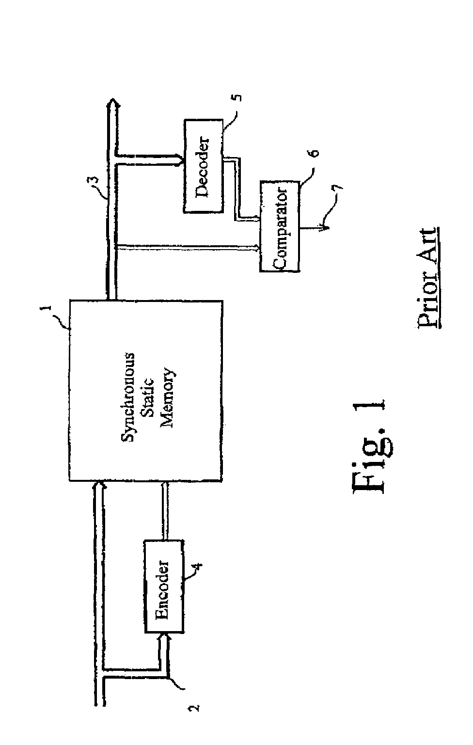
Thus, it can be noted that static storages whose load capacities are increasingly lower with the development of technologies, become particularly sensitive to electromagnetic fields and disturbances, which obviously is an important source of errors disturbing correct operation of electronic circuits.
However, it is noted that the use of such a system usually penalizes the system's operating speed.
Thus memory circuits functioning at high speed are not adapted to use an error correcting code, which is very regrettable since nowadays many applications are used for which operating speed goes hand in hand with data integrity and security.

Method used


Image

  • Memory circuit comprising an error correcting code
  • Memory circuit comprising an error correcting code
  • Memory circuit comprising an error correcting code

Examples


second embodiment

[0044]The second embodiment is illustrated in FIG. 3 and comprises a first single port RAM 200—with a size allowing to store 24K words of 32 bits each, for example—and a second double port memory 230—for example with a size of 24K×7—dedicated to the recording of error correcting codes.

[0045]RAM 200 has an address bus (A), a data bus (D) and a control bus comprising in particular the Write Enable signal. Output data Dout32 is available on a bus 215.

[0046]Referring now the input bus RAM 200, it can be seen that the data bus (D) of RAM 20 receives information Din32SP from a first multiplexer 217 via a bus 218. Multiplexer 217 has two input buses. A first input of multiplexer 217 receives data to be stored (DIN32) transmitted by a processor (not shown) via a bus 208, and a second input receives information C-Dout32 provided by an EEC-decoder 226. As will be explained later, multiplexer 217 makes it possible to deliver the corrected value computed by circuit 226 to memory 200 where the n...

third embodiment

[0054]Referring to FIG. 5, a memory circuit will now be described, wherein the double port memory is replaced with a less expensive single port memory.

[0055]The circuit comprises a first RAM 300 and a second memory 330, both memories being with single port memories. The first memory is dedicated to data recording while the second one is dedicated to error correcting codes recording.

[0056]RAM 300 has a data bus (D) receiving information DIN32SP from a first multiplexer 317 via a bus 318. Multiplexer 317 has two input buses. A first input receives the data to be stored (DIN32) available on a bus 308, while a second input receives information C-Dout32 provided by an EEC-decoder 326 similar to circuit 226 of FIG. 3. As previously, multiplexer 317 makes it possible to deliver the corrected value computed by circuit 326 to the input of memory 200 in order to rewrite the new corrected value in memory. Control WEN of RAM 300 receives a control signal WENSP transmitted via a circuit 320, whi...


PUM


Abstract

A memory circuit with an error correcting system comprising an address bus (102), an input data bus (108), and an output data bus (115), the circuit comprising a memory having an address bus (113), a data bus (114) and an error correcting circuit comprising an encoder (107). A first address register (104) is connected to the input address bus of the circuit for successively storing addresses corresponding to memory write operations only. A second data register (105) is connected to the input data bus of the circuit (108) for storing data transmitted to the encoder (107). Circuits make it possible to introduce a one-cycle shift into the memory writes, without modifying reads, giving the encoder more time to compute error correcting codes.

Description

CROSS-REFERENCE TO RELATED APPLICATION[0001]This application is based upon and claims priority from prior French Patent Application No. 02 06794, filed on Jun. 3, 2002, the entire disclosure of which is herein incorporated by reference.BACKGROUND OF THE INVENTION[0002]1. Field of the Invention[0003]The present invention relates to memory circuits, and in particular to a memory circuit equipped with an error correcting code system.[0004]2. Description of the Related Art[0005]With the continuous growth of their computing power and the rise of their operation frequency, the sensitivity of information processing systems to errors likely to corrupt data considerably increases. This is all the more sensitive since miniaturization of electronic components reduces the size of the electronic components contained in Very Large Systems Integration (V.L.S.I.) circuits and in particular the size of Read Access Memory (R.A.M) circuits integrated therein.[0006]Thus, it can be noted that static sto...

Claims


Application Information

Patent Timeline
IPC IPC(8): G11C29/42G06F11/10
CPCG06F11/1008G06F11/1048
Inventor JACQUET, FRANCOISSCHOELLKOPF, JEAN-PIERRE
Owner STMICROELECTRONICS SRL
Features
  • R&D
  • Intellectual Property
  • Life Sciences
  • Materials
  • Tech Scout
  • Unparalleled Data Quality
  • Higher Quality Content
  • 60% Fewer Hallucinations
Learn More