Microstrip stabilized quantum well resonance-tunneling generator for millimeter and submillimeter wavelength range

a quantum well resonance and generator technology, applied in oscillator generators, semiconductor/solid-state device details, semiconductor devices, etc., can solve the problems of reducing the output power achieved in such systems at shorter wavelengths, and affecting the efficiency of resonant tunneling diodes

Active Publication Date: 2007-09-25
SAMSUNG ELECTRONICS CO LTD +1
View PDF1 Cites 3 Cited by
  • Summary
  • Abstract
  • Description
  • Claims
  • Application Information

AI Technical Summary

Benefits of technology

[0017]A monolithic integrated construction of the generator device of the present invention allows the application of the methods of molecular beam epitaxy and thin-film epitaxy. The present invention allows achievement of a minimum level of electrical losses and an optimal wave impedance matching system in short millimeter wavelength range. A high speed of the resonant tunneling diodes combined with the possibility of the optimal matching of the wave impedance provided by microstrip resonator systems of the present invention is promising for application in short millimeter and submillimeter wavelength ranges.
[0022]the choice of the optimal design of the generator using high-speed quantum semiconductor heterostructures providing the optimal wave impedance matching of the active element and resonator as well as decreasing the parasitic inductance and optimizing parameters of electric circuitry in millimeter and submillimeter wavelength ranges;
[0025]the development of the multiplying technology of fabrication of the device including multiple generator units with the aim of increasing its output power and decreasing manufacturing costs; and / or
[0027]The present invention is directed to solving the task of increasing the oscillation frequency of solid state microwave generator towards the terahertz frequency range. According to the present invention, elements of the generator device are manufactured using a monolithic integrated construction such that the elements are fabricated on a common substrate allowing the application of the methods of molecular beam epitaxy and thin-film epitaxy. The present invention may achieve:
[0031]the reducing of the overall dimensions, the weight and the lowering manufacturing costs; and / or
[0035]With the aim of improving the output power of the device, a series of resonant tunneling diodes connected with microstrip lines may be located on the same substrate in configuration providing the optimal phase relations for generated electromagnetic wave.

Problems solved by technology

In spite of extremely high speed of electronic charge transfer processes in resonant tunneling nanostructures the achievement of terahertz frequencies in resonant tunneling diode based generators is rather difficult due to the problems in fabricating the high-Q three-dimensional confined cavity resonators for this wavelength range, as well as providing proper circuit conditions in interconnecting the external resonator and resonant tunneling diode.
In particular, the waveguide systems, which are extremely effective in the microwave range cease to work at short millimeter and submillimeter wavelengths due to an increase of the energy losses in metallic elements.
This results in a considerable decrease of the output power achieved in such systems at shorter wavelengths.
This is rather difficult to achieve when the active element and the resonator are fabricated separately.

Method used


Image

  • Microstrip stabilized quantum well resonance-tunneling generator for millimeter and submillimeter wavelength range
  • Microstrip stabilized quantum well resonance-tunneling generator for millimeter and submillimeter wavelength range
  • Microstrip stabilized quantum well resonance-tunneling generator for millimeter and submillimeter wavelength range

Examples


Embodiment Construction

[0041]Hereinafter, the present invention will be described in detail with reference to the drawings.

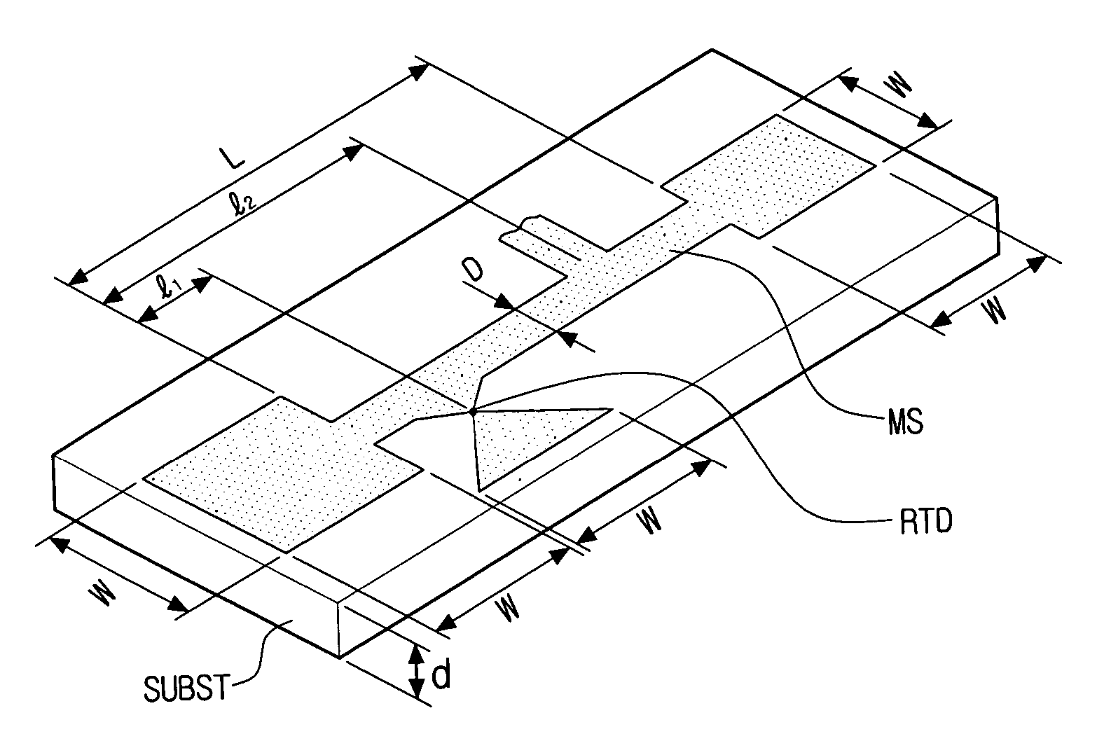
[0042]According to the present invention, a microstrip generator in monolithic integrated design comprises the resonant-tunneling diode structure with quantum wells and barriers, grown on semi-insulating substrate of GaAs, which is used simultaneously as a dielectric layer of the microstrip line. Both the resonant tunneling structure and the microstrip lines are fabricated using a common technological process including MBE growth of the layers of the structure and photolythographic formation of a resonant-tunneling diode, a microstrip resonator and interconnecting lines and contact junctions. The exemplary embodiments of the present invention are operable in a frequency range order of 300 GHz (wavelength of 1 mm).

[0043]FIG. 1 is a view of a microstrip stabilized quantum-well resonance-tunneling generator for short millimeter wavelength range according to an exemplary embodiment of the...


PUM


Abstract

A microstrip stabilized quantum well resonance-tunneling generator which generates electromagnetic waves for millimeter and submillimeter wavelength range is provided The generator includes a resonant tunneling semiconductor quantum well diode, and a microstrip resonator. The resonant tunneling diode, the microstrip resonator and interconnecting lines and junctions are fabricated as a monolithic integrated device on a common substrate. As a result, the monolithic integrated device provides the expansion of the operation frequency range toward the terahertz region as a result of reduction of the parasitic inductance as well as of minimizing the other parasitic parameters of the electric circuitry connecting the resonant tunneling diode and resonator.

Description

CROSS-REFERENCE TO RELATED APPLICATION[0001]This application claims priority from Russian Patent Application No. 2004125910 filed Aug. 25, 2004 in the State Patent Office of the Russian Federation, and Korean Patent Application No. 2005-62965 filed Jul. 12, 2005 in the Korean Intellectual Property Office, the entire contents of which are incorporated herein by reference.BACKGROUND OF THE INVENTION[0002]1. Field of the Invention[0003]The present invention relates to the fields of microwave signal sources, solid state high-frequency electronics and microelectronics. More particularly, the present invention relates to a microstrip stabilized quantum well resonance-tunneling generator which generates electromagnetic waves of millimeter and submillimeter wavelength range.[0004]2. Description of the Prior Art[0005]Quantum effects including resonant tunneling effects are widely used in modern solid state and semiconductor electronics for application in the fields of communications, radiovi...

Claims


Application Information

Patent Timeline
Patent Type & Authority Patents(United States)
IPC IPC(8): H03B5/18
CPCB82Y10/00H01P1/005H01P7/082H03B7/08H03B7/14
Inventor KAZAKOV, IGOR PETROVICHKARUZSKY, ALEXANDER LVOVICHMITYAGIN, YURY ALEKSEEVICHMURZIN, VLADIMIR NIKOLAEVICHTSHOVREBOV, ANDREY MICHAYLOVICH
Owner SAMSUNG ELECTRONICS CO LTD
Why Eureka
Try Eureka