LED with series-connected monolithically integrated mesas

a monolithic, series-connected technology, applied in the field of lighting arts, can solve the problems of reducing light conversion efficiency, reducing the efficiency of low voltage devices, and limiting the spatial separation between power sources and light emitting diodes, so as to achieve the effect of increasing system complexity

Active Publication Date: 2007-10-23
GE LIGHTING SOLUTIONS LLC
View PDF12 Cites 225 Cited by
  • Summary
  • Abstract
  • Description
  • Claims
  • Application Information

AI Technical Summary

Benefits of technology

[0012]One advantage resides in improved uniformity of current distribution in the light emitting diode die.
[0013]Another advantage resides in substantial reduction in hotspots due to reduced current bunching.
[0014]Another advantage resides in providing substantially uni-directional current flow for a series-interconnected set of light emitting diode mesas on a device die. The unidirectional current flow provides a short total current path length for a series-interconnected set of light emitting diode mesas on a device die, which in turn reduces resistive power losses and increases device robustness.
[0015]Another advantage resides in improved robustness against localized defects due to a wide or elongated current distribution transverse to the current flow direction.

Problems solved by technology

Low voltage devices have certain disadvantages at the system level.
Since resistive power losses scale with current-squared, increasing current can reduce light conversion efficiency.
Moreover, since interconnect voltage drops per unit length of wire or printed circuit trace increases proportionally with current, high operating currents can limit the spatial separation between the power source and the light emitting diode.
At the die level, low voltage operation is also problematic.
However, resistive voltage drops generally do not substantially increase light output intensity, since some of the energy is going into resistive heating.
Furthermore, the resistive heating can increase the resistivity of the semiconductor materials, further exasperating the resistance problem.
Resistive heating can produce other undesirable effects such as thermal device failure.
In summary, the low voltage, high current nature of light emitting diodes limits the magnitude of light output that can be achieved with a single diode junction.
However, such component-level series interconnection increases system complexity and produces a spatially distributed light source.
Additionally, failure of one device in the series breaks the current path and can cause failure of the entire series-interconnected chain of light emitting diodes.
However, these light emitting diode devices have certain disadvantages.
The devices typically exhibit non-uniform current distribution because current is injected from the mesa side and spreads non-uniformly over the mesa area.
Such current non-uniformity can reduce light output efficiency and can introduce thermal hotspots.
Moreover, the entire device die may degrade in performance or catastrophically fail due to a current flow problem with any single mesa, or with any single series interconnection in the series-interconnected chain of light emitting diode mesas.
A relatively long overall current path of the device also leads to increased resistive voltage drop, increased resistive current-squared power losses, and consequent reduction in light output efficiency.
Still further, the electrodes of the die are relatively large to accommodate the power input needed to drive the plurality of mesas in series, and these large electrodes are disposed outside the light emitting area, which substantially reduces the active area of the light emitting diode die.

Method used


Image

  • LED with series-connected monolithically integrated mesas
  • LED with series-connected monolithically integrated mesas
  • LED with series-connected monolithically integrated mesas

Examples


Embodiment Construction

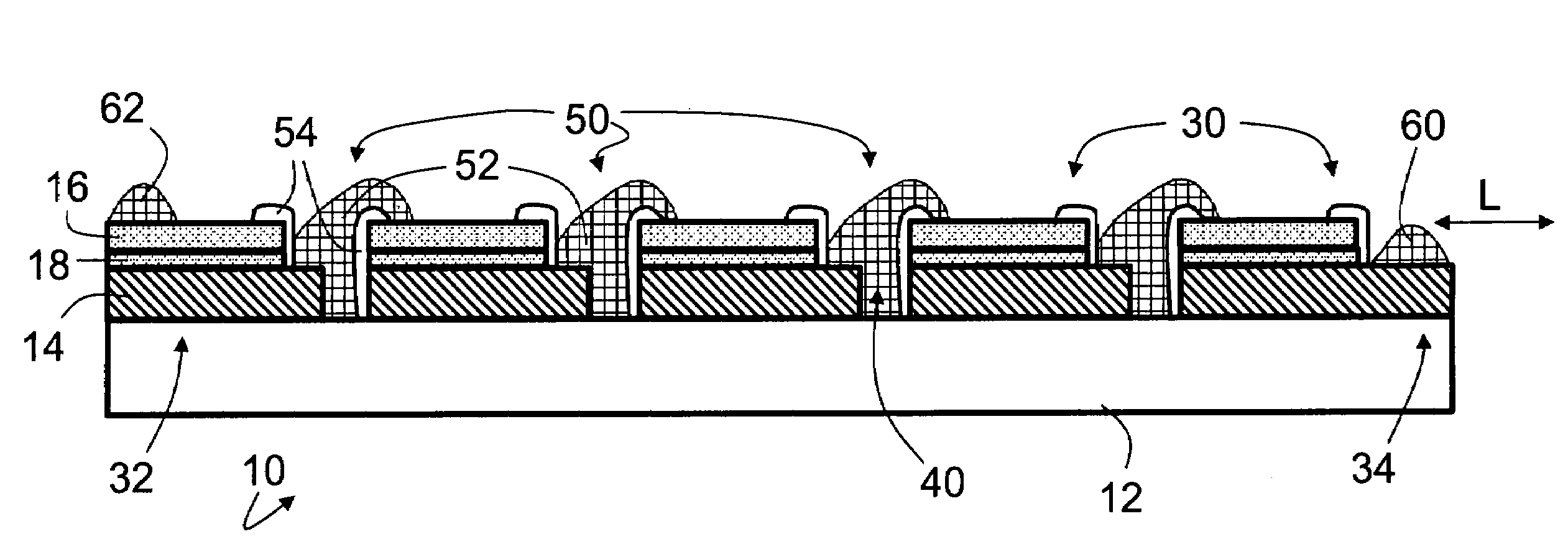
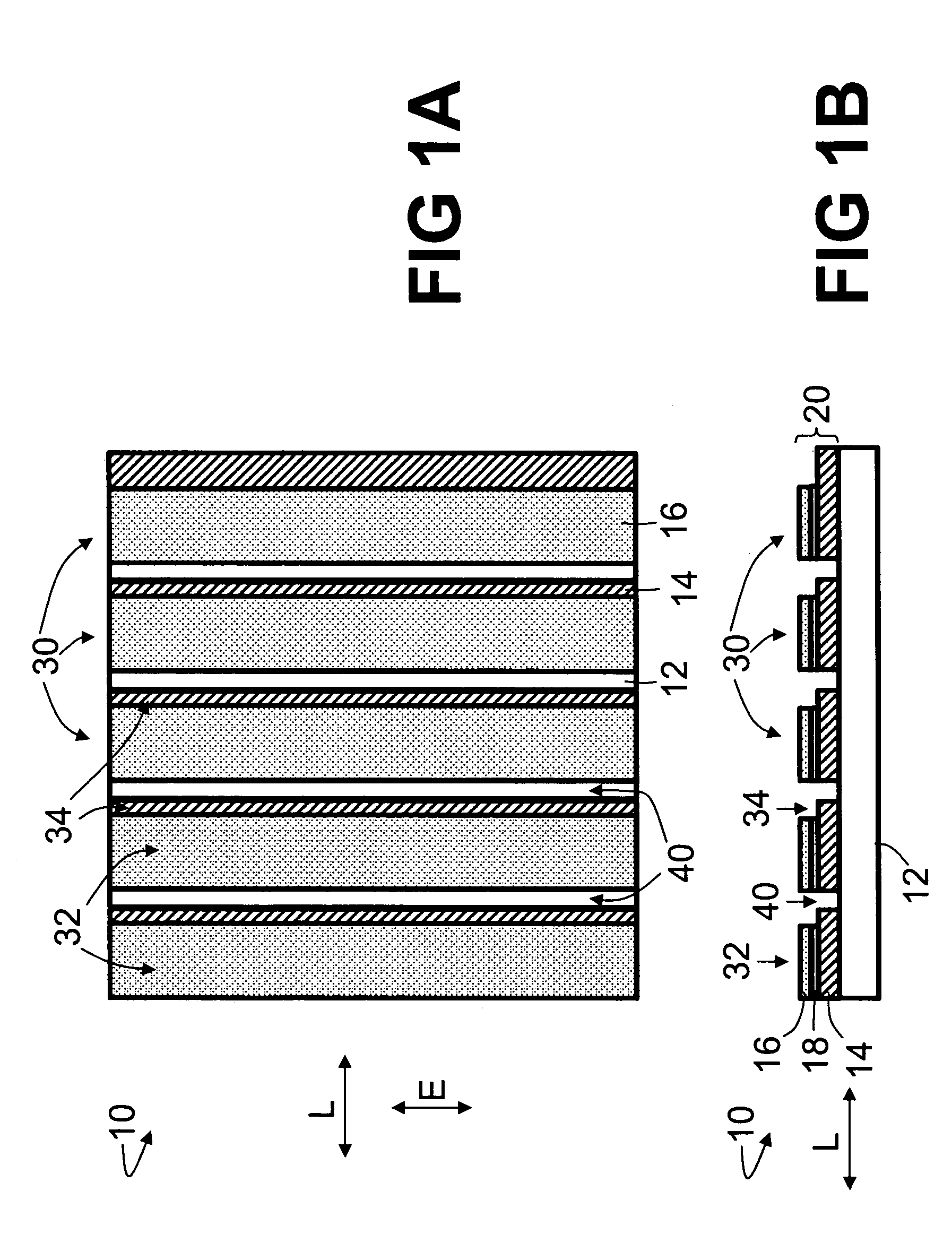
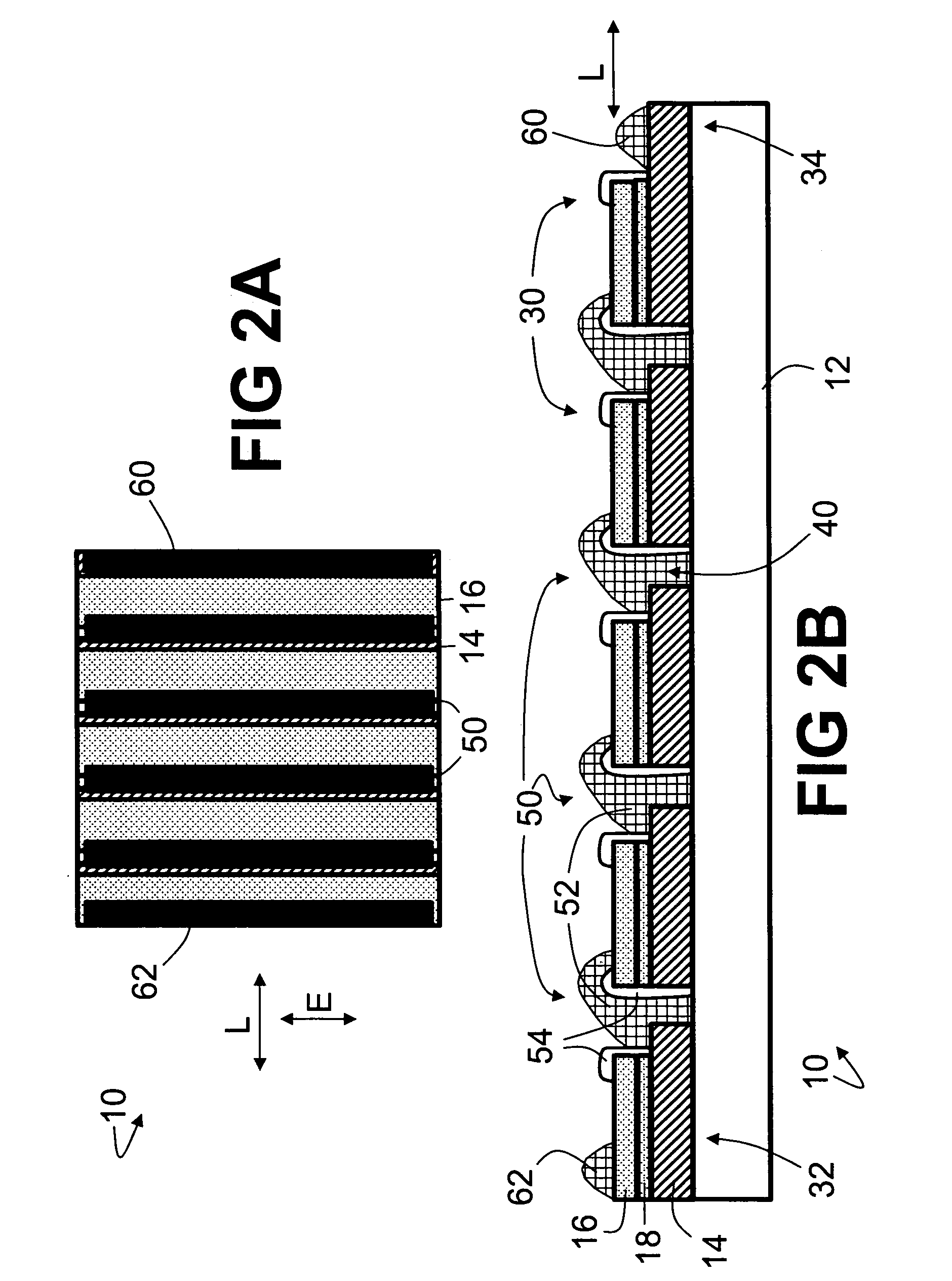
[0026]With reference to FIGS. 1A and 1B, a light emitting diode die 10 includes a substrate 12, a first conductivity type layer 14 disposed between the substrate 12 and a second conductivity type layer 16, and an active region 18 disposed between the first and second conductivity type layers 14, 16. The first and second conductivity type layers 14, 16 and the active region 18 are collectively referred to herein as a device layers stack 20. In one embodiment, the substrate 12 is a sapphire, silicon carbide, or gallium nitride substrate, and the device layers stack 20 is principally made up of group III-nitride layers such as gallium nitride layers, aluminum nitride layers, indium nitride layers, and ternary and quaternary compounds thereof. In another embodiment, the substrate 12 is gallium arsenide or indium phosphide, and the device layers stack 20 is principally made up of group III-arsenide and / or group III-phosphide layers. Other semiconductor materials can also be used for the ...


PUM


Abstract

A light emitting semiconductor device die (10, 110, 210, 310) includes an electrically insulating substrate (12, 112). First and second spatially separated electrodes (60, 62, 260, 262, 360, 362) are disposed on the electrically insulating substrate. The first and second electrodes define an electrical current flow direction directed from the first electrode to the second electrode. A plurality of light emitting diode mesas (30, 130, 130′, 230, 330) are disposed on the substrate between the first and second spatially separated electrodes. Electrical series interconnections (50, 150, 250, 350) are disposed on the substrate between neighboring light emitting diode mesas. Each series interconnection carries electrical current flow between the neighboring mesas in the electrical current flow direction.

Description

BACKGROUND[0001]The present invention relates to the lighting arts. It especially relates to light emitting diodes with inverted flip-chip orientations, and will be described with particular reference thereto. However, the invention will also find application in conjunction with non-inverted light emitting diodes, laser diodes, and the like.[0002]Light emitting diodes are generally low voltage devices having operating voltages of a few volts. For example, a typical gallium nitride-based light emitting diode has a forward operating voltage of about 3-4 volts. Low voltage devices have certain disadvantages at the system level. Voltage dividers, power regulators, or other power conditioning circuitry may be needed to reduce high voltage electrical power to a level suitable for driving the light emitting diodes. Moreover, the low voltage calls for relatively high operating current to achieve high brightness. Since resistive power losses scale with current-squared, increasing current can...

Claims


Application Information

Patent Timeline
Patent Type & Authority Patents(United States)
IPC IPC(8): H01L33/00H01L21/00H01L27/15H01L33/20
CPCH01L27/153H01L33/20H01L33/62H01L2924/0002H01L2924/00
Inventor ELIASHEVICH, IVANBOHLER, CHRISSHELTON, BRYAN S.VENUGOPALAN, HARI S.GAO, XIANG
Owner GE LIGHTING SOLUTIONS LLC
Why Eureka
Try Eureka