Application of acoustic and vibrational energy for fabricating bumped IC die and assembly of PCA's

a vibration and vibration energy technology, applied in the direction of soldering apparatus, lighting and heating apparatus, liquid cleaning, etc., can solve the problems of high assembly cost, high assembly cost, and inability to manufacture bumped ic wafers or dies, and achieve the effect of low cost and repeatability

Inactive Publication Date: 2007-11-13
HERTZ ALLEN DAVID +2
View PDF14 Cites 13 Cited by
  • Summary
  • Abstract
  • Description
  • Claims
  • Application Information

AI Technical Summary

Benefits of technology

[0043]The acoustic energy applied to solder paste during the process of separating the stencil and the PCB increases the separation of the solder paste from within the solder stencil aperture.
[0075]The present invention further combines the enhancements of the print release portion of the present invention, the cleaning portion of the present invention, and the drying portion of the present invention. The combination of at least two of the contributors directs a method and apparatus forward for utilizing screen printing technology for applying solder bumps to IC Die or wafers, resulting in a repeatable, low cost solution.

Problems solved by technology

The current process for applying solder bumps to IC wafers or die is extremely inefficient resulting in high assembly costs.
The screen printing process is made more difficult as the size of the apertures decreases and the size of the surface area on the objects decreases.
First, the deposited material may slump or otherwise move outside the area defined by the aperture after the stencil is removed.
For electronic assemblies, this can have disastrous consequences and require rework of defects.
Secondly, the shape of the remaining material may cause problems.
This is generally due to shrinkage in the size of the components to be mounted or the density of the leads of the components.
As mentioned earlier, the material may slump and migrate outside the area defined by the aperture causing conductivity problems.
Further, the surface area of the resulting deposit may not be uniform (illustrated later), potentially creating problems in attaching components.
The detriment of this approach is that it inherently increases the cycle time of the process.
The limitations of this process continue to be challenged with the inclusion of smaller openings within connectors, smaller gaps under components, and the like which can entrap moisture.
Any excess water or moisture will cause corrosion over time.
This is especially a problem when power is applied to a module which is not dry, causing a galvanic reaction and, therefore, corrosion.
If the solder paste dries within the apertures of the stencil, the dried solder paste will interfere with the release of the solder paste during the next assembly process and cause defects.
Solder stencils are not currently used for applying solder paste or solder spheres to IC Wafers, as the cleaning process is very time consuming as well as incomplete.
Build up of flux residue on wave solder pallets will hinder the application of the flux onto the assembly and cause defects.
The under wiping process may not sufficiently remove excess solvent remaining on the top-side of the stencil.
The process may not remove the solder residue within the apertures of the stencil.
Chemicals with relatively low flash points were used in the past, but those chemicals are expensive and some were found to be harmful to the environment.
Water, or other cleaning solutions with similar flash points, is difficult to dry in a short time period.
The limitations of this are that the dryers require a great deal of thermal energy and large capacity air blowers to provide sufficient drying.
Additionally, these dryers are generally loud and require sound dampening.
The last few points of moisture removal take the longest and increase the cost of drying.
If one attempts to increase the temperature of the drying gas, there is a risk of thermally damaging the electronic components on the module.
Thermally damaging the module sets a practical upper limit for the gas temperature.
Additionally, this process continues to be limited when moisture is trapped in components such as connectors.
This process is somewhat limited by the time required to dry any excess moisture.
Solder Stencil printers do not have any known means of drying other than the paper used to wipe the underside of the stencil, and the under wipe paper is not conducive to removing moisture.
The limitations of this patent are that electronic modules cannot be tumbled in a drum and are most often processed on a conveyor to preclude damage to the module.
This type of dryer would not work with electronic modules as any stirring of electronic modules would cause mechanical damage to the modules.
While each of these improvements has contributed to the art, the limitations of these processes continue to be challenged.

Method used


Image

  • Application of acoustic and vibrational energy for fabricating bumped IC die and assembly of PCA's
  • Application of acoustic and vibrational energy for fabricating bumped IC die and assembly of PCA's
  • Application of acoustic and vibrational energy for fabricating bumped IC die and assembly of PCA's

Examples


Embodiment Construction

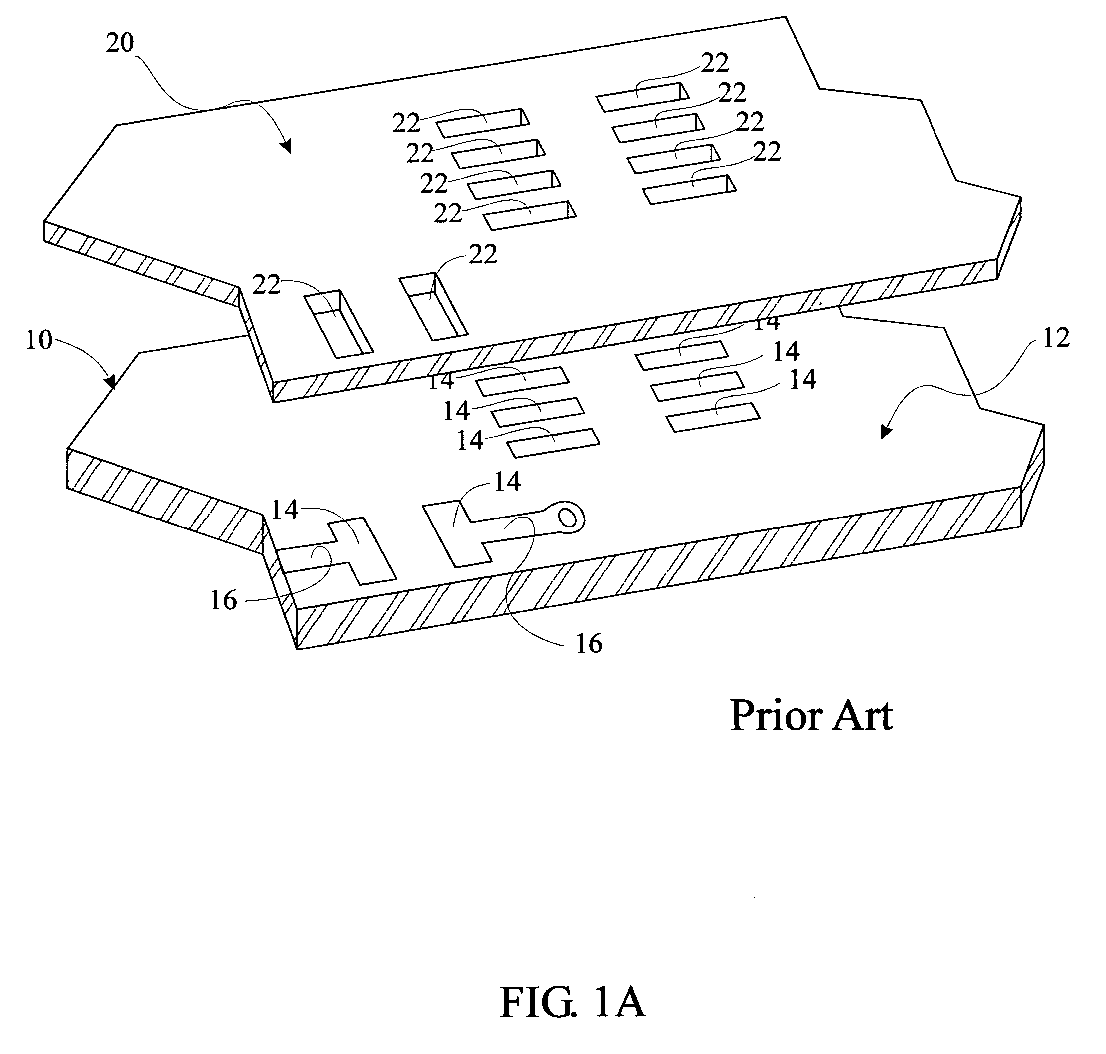
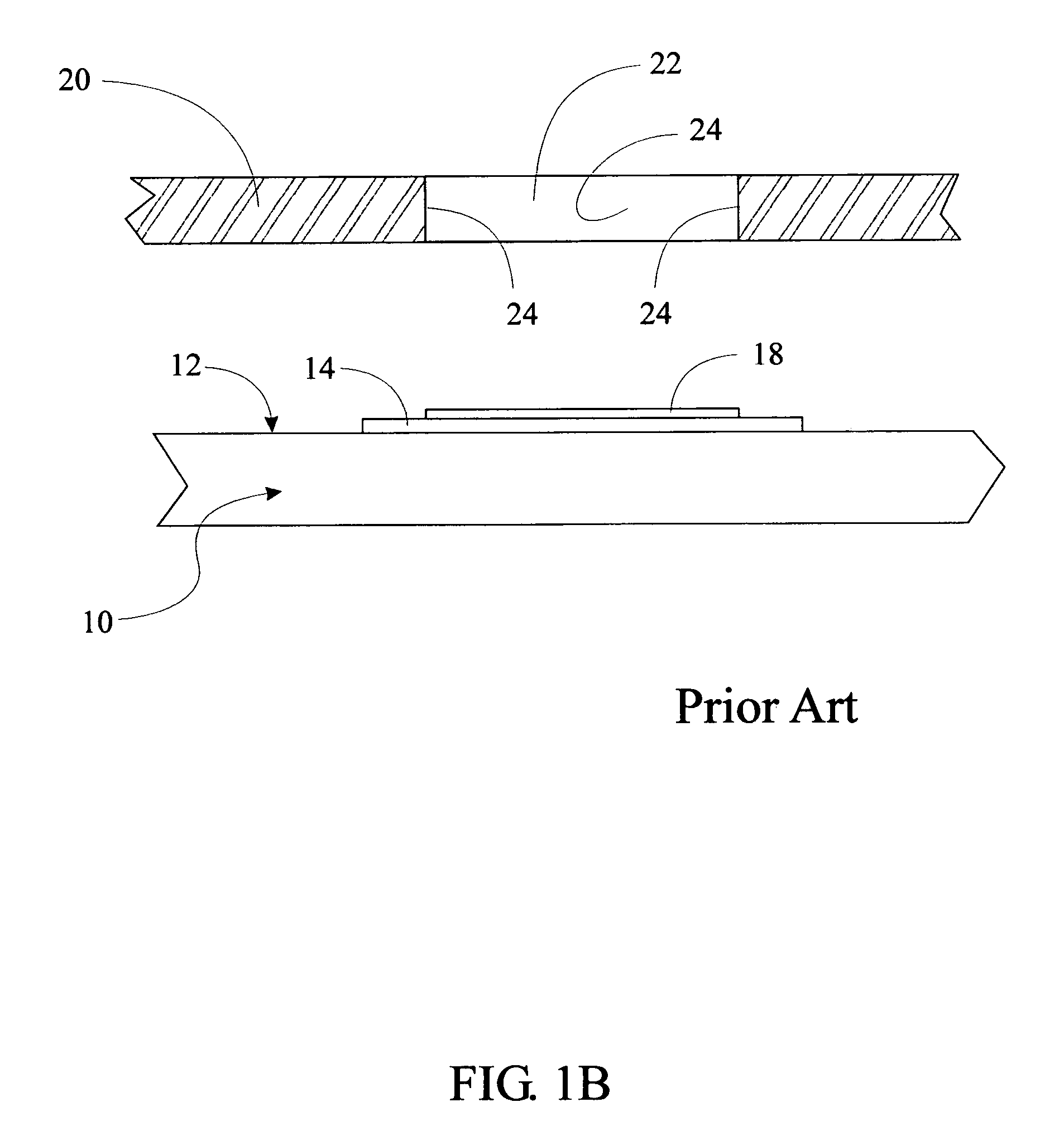
[0095]FIG. 3 is a flow diagram showing the preferred screen printing steps of the present invention. FIGS. 1B, 1C and 1D illustrate some of the steps in the process. The first step 60 is the fabrication of a screen or stencil 20. A stencil is a sheet like device created by fashioning apertures into a foil. Stencils may be fabricated using many methods that are known in the art including but not limited to, precision milling of a raw foil preferably using a programmable computer controlled mill, chemically etching using photodeveloped or equivalent masking images on a raw foil and applying a predetermined chemical which will corrosively remove the exposed portions of the foil, an additive process which uses a negative pattern and bonds particles of metal around the pattern to form a foil, or laser cutting using a programmable, focused laser beam to cut through the foil.

[0096]The second step 62 in the preferred screen printing process is to align a Printed Circuit Board 10 in a manner...


PUM

PropertyMeasurementUnit
aspect ratioaaaaaaaaaa
vibrational energyaaaaaaaaaa
vibrationalaaaaaaaaaa

Abstract

A method and apparatus are disclosed for improving a screen printing process by applying vibrational energy to assist in the print release, cleaning, and drying processes. The vibrational energy or acoustic pressure waves may be created by a transducer where the waves are transferred to the stencil or printable material through air or a vibrational interface medium. The vibrational energy in turn assists with separating the printable material from the side walls of the apertures of the stencil. The vibrational energy can further assist in the process of cleaning the stencil. The acoustic pressure can also be used in the drying process by having the waves impinge on the water droplets to atomize the droplets on the surface of the stencil. The technology can be used for the assembly of Printed Circuit Assemblies, Ball Grid Array IC Packages, Flip Chip, etc. The same technology may be applied to other cleaning processes for cleaning Printed Circuit Assemblies, tooling, and the like, whereby the cleaning processes can assist in cleaning within the cracks, crevices and hard to reach areas of connectors and other components, without undesirable heat.

Description

RELATED US APPLICATION DATA[0001]This patent application claims priority to Utility application Ser. No. 09 / 621,249, filed Jul. 21, 2000 (Issuing as U.S. Pat. No. 6,662,812) which claims priority to Provisional Patent Application 60 / 145,524 filed Jul. 24, 1999.[0002]This patent application further claims priority to Utility patent application Ser. No. 09 / 208,959, filed on Dec. 10, 1998 (Issued as U.S. Pat. No. 6,138,562) which claims priority to U.S. Provisional Application No. 60 / 071,866, filed Jan. 20, 1998[0003]This patent application further claims priority to Utility patent application Ser. No. 09 / 309,697 filed on May 11, 1999, (issued as U.S. Pat. No. 6,412,685) which is a continuation-in-part of Ser. No. 08 / 789,883 filed 1997, Jan. 28 (issued as U.S. Pat. No. 6,202,918).[0004]All of the above are incorporated by reference.FIELD OF THE INVENTION[0005]This invention relates in general to the field of screen printing, and in particular to a method and apparatus for acoustic and ...

Claims


Application Information

Patent Timeline
Patent Type & Authority Patents(United States)
IPC IPC(8): B08B3/10B08B7/02B41F35/00F26B5/02F26B5/12H05K3/12H05K3/22H05K3/26
CPCB08B7/028B41F35/005F26B5/12H05K3/227F26B5/02B41P2235/14H05K3/26H05K3/1216
Inventor HERTZ, ALLEN DAVIDHERTZ, ERIC LEEEPP, DENNIS D.
Owner HERTZ ALLEN DAVID
Why Eureka
Try Eureka