Semiconductor device

a semiconductor device and main circuit technology, applied in the direction of electric variable regulation, process and machine control, instruments, etc., can solve the problems of increase in switching loss, etc., to achieve the effect of enhancing power supply efficiency of semiconductor devices, and reducing parasitic inductance of main circuit in power supply circui

Inactive Publication Date: 2007-11-13
RENESAS ELECTRONICS CORP
View PDF7 Cites 37 Cited by
  • Summary
  • Abstract
  • Description
  • Claims
  • Application Information

AI Technical Summary

Benefits of technology

[0018]Advantageous effects obtained by representatives of the inventions disclosed in the present application will briefly be explained as follows:
[0019]A field effect transistor of a first semiconductor chip is formed of a p channel vertical field effect transistor, and a field effect transistor of a second semiconductor chip is formed of an n channel vertical field effect transistor, whereby the first and second semiconductor chips are mounted over the same chip mounting section and electrically connected to each other. Thus, since inductance components in a wiring path between the first and second semiconductor chips can be reduced, parasitic inductance of a main circuit in a power supply circuit can be reduced.
[0020]A capacitor has a pair of electrodes whose one is bonded to the first lead plate and whose other is bonded to the second lead plate. Thus, since parasitic inductance of a main circuit in a power supply circuit can be reduced, power supply efficiency of a semiconductor device can be enhanced.

Problems solved by technology

However, a problem arises in that a loss increases due to main circuit inductance parasitic on a main circuit around the input capacitor of the non-insulated DC-DC converter under the large-current and high-frequency conditions.
In particular, a problem arises in that when the main circuit inductance parasitic on the main circuit around the input capacitor increases with the increases in current and frequency, a leap voltage at the turning off of the high-side power MOS•FET of the DC-DC converter increases, thus resulting in an increase in switching loss and the incurrence of large loss.
In such a configuration, however, parasitic inductance cannot be reduced sufficiently because the source of the high-side power MOS•FET an the drain of the low-side power MOS•FET are connected by the bonding wire.

Method used


Image

  • Semiconductor device
  • Semiconductor device
  • Semiconductor device

Examples


first preferred embodiment

[0088]A semiconductor device according to a first embodiment is a non-insulated DC-DC converter employed in a power supply circuit of electronic equipment like, for example, a desktop personal computer, a notebook-size personal computer, a server or a game machine or the like.

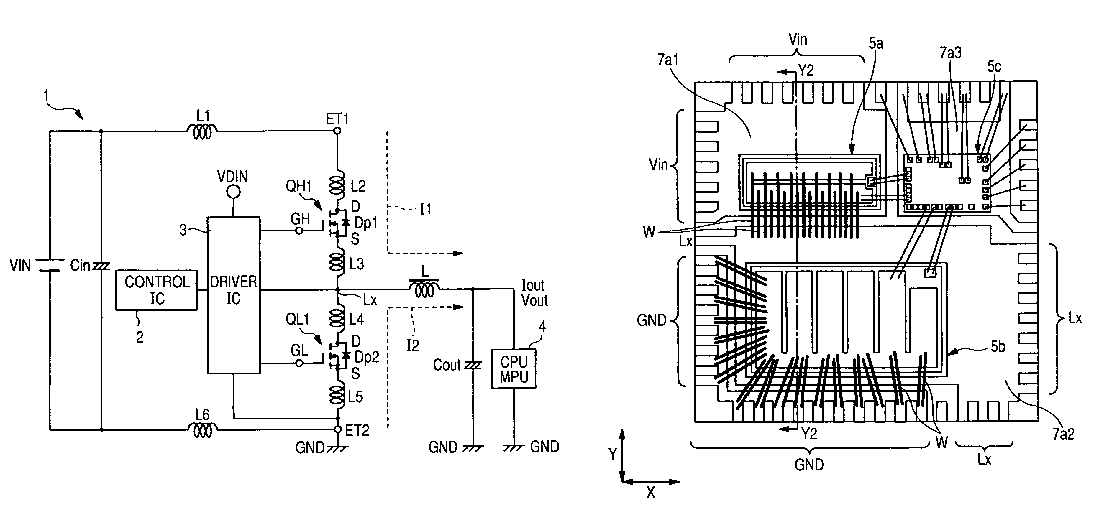
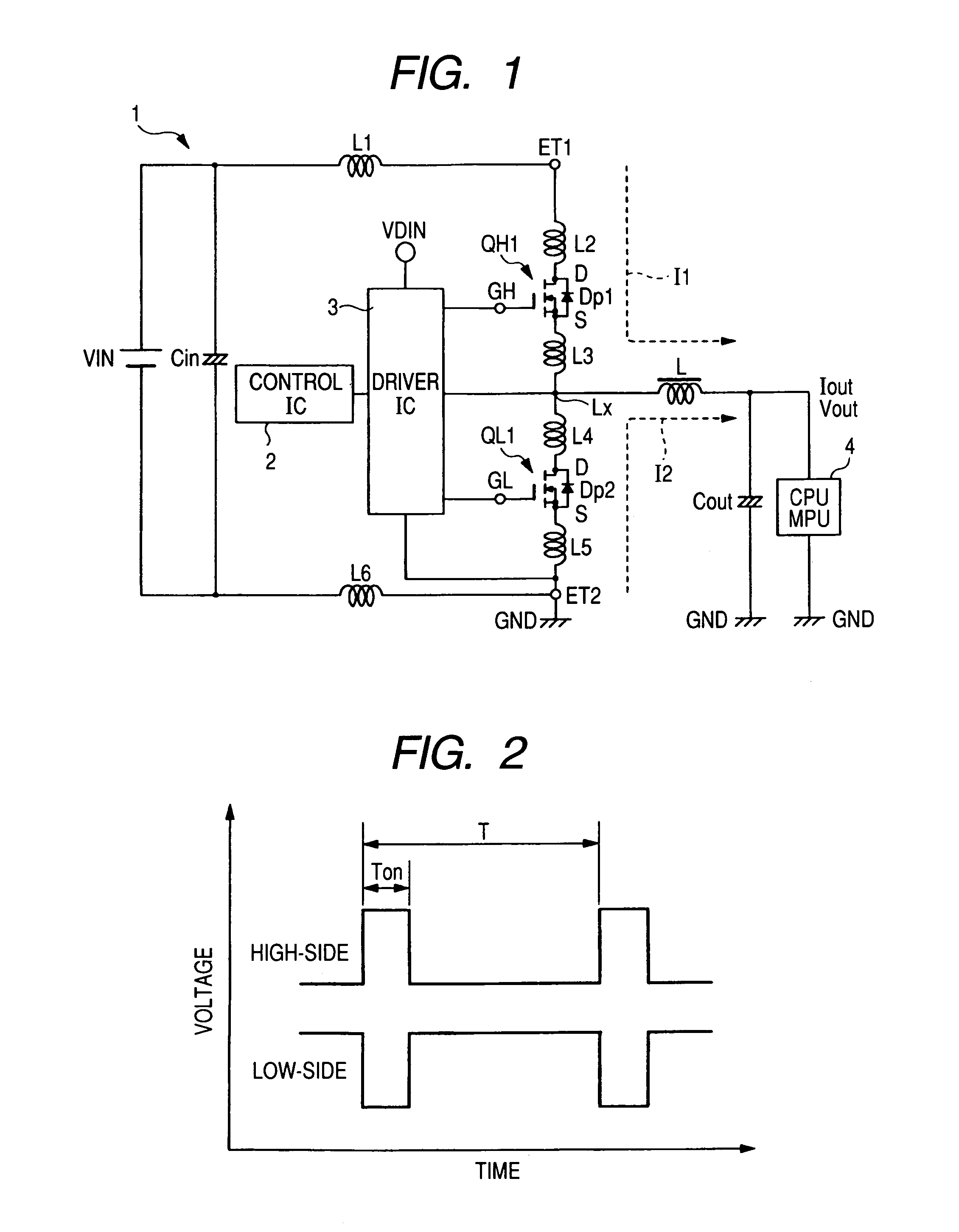
[0089]FIG. 1 shows one example of a circuit diagram of a non-insulated DC-DC converter 1 discussed by the present inventors. The non-insulated DC-DC converter 1 has elements like a control circuit 2, a driver circuit 3, power MOS•FETs (hereinafter abbreviated simply as “power MOS”) QH1 and QL1, an input capacitor Cin, an output capacitor Cout and a coil L, etc. Incidentally, symbol D indicates a drain, and symbol S indicates a source, respectively. Symbols L1 through L6 indicate parasitic inductances which are parasitic on a main circuit of the non-insulated DC-DC converter.

[0090]The control circuit 2 is a circuit like, for example, a pulse width modulation (Pulse Width Modulation: PWM) circuit or the like, whi...

second preferred embodiment

[0131]A second embodiment will explain a case in which an n channel horizontal power MOS is used for a high-side power MOS of a non-insulated DC-DC converter. While the present embodiment is identical to FIG. 1 in circuit diagram, each p+ type punch-out layer is used in the n channel horizontal power MOS. Thus, such a configuration that a drain electrode is disposed in a main surface of a semiconductor chip and a source electrode is disposed in a back surface of the semiconductor chip, is taken. Therefore, a die pad can be shared between a high-side power MOS and a low-side power MOS in a similar to the use of the p channel vertical power MOS as in the first embodiment. It is thus possible to reduce the parasitic inductances L3 and L4. The parasitic resistance of each wiring that electrically connects the source of the high-side power MOS and the drain of the low-side power MOS can also be reduced. In the high-side power MOS, switching losses (turn-on loss and turn-off loss) look la...

third preferred embodiment

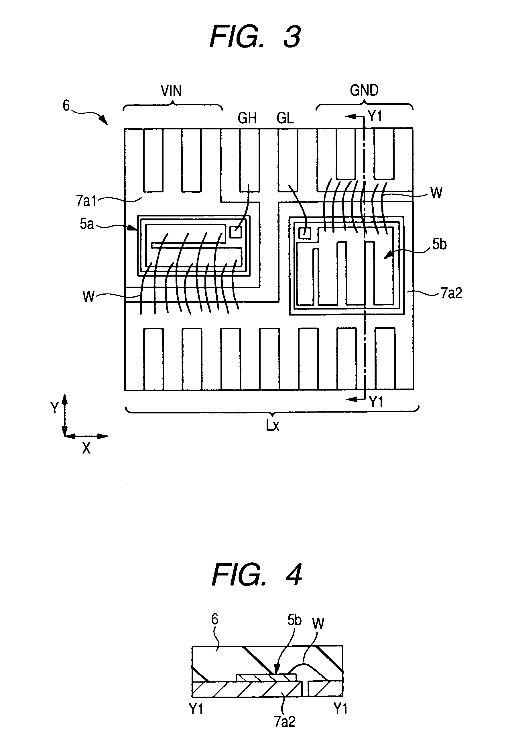
[0137]A third embodiment will explain a configuration wherein three semiconductor chips constituting a non-insulated DC-DC converter are accommodated within one package.

[0138]FIG. 18 shows an overall plan view illustrating a main surface side of a package 10B employed in the third embodiment, FIG. 19 shows a side view of the package 10B shown in FIG. 18, and FIG. 20 shows an overall plan view illustrating a back surface side of the package 10B shown in FIG. 18, respectively.

[0139]The package 10B of the third embodiment is provided as a QFN (Quad Flat Non-leaded package) configuration, for example. However, the package 10B is not limited to the QFN configuration and can be changed in various ways. The package 10B may be formed as a flat package configuration like, for example, a QFP (Quad Flat Package), an SOP (Small Out-line Package) or the like.

[0140]An encapsulator 6 that constitutes the package 10B has an outward appearance shaped in the form of a thin plate. Back surfaces of two...


PUM


Abstract

The object of the present invention is to reduce parasitic inductance of a main circuit in a power supply circuit. The present invention provides a non-insulated DC-DC converter having a circuit in which a power MOS• FET for a high-side switch and a power MOS•FET for a low-side switch are connected in series. In the non-insulated DC-DC converter, the power MOS•FET for the high-side switch is formed by a p channel vertical MOS•FET, and the power MOS•FET for the low-side switch is formed by an n channel vertical MOS•FET. Thus, a semiconductor chip formed with the power MOS•FET for the high-side switch and a semiconductor chip formed with the power MOS•FET for the low-side switch are mounted over the same die pad and electrically connected to each other through the die pad.

Description

CROSS-REFERENCE TO RELATED APPLICATION[0001]The present application claims priority from Japanese patent application No. 2004-345798 filed on Nov. 30, 2004, the content of which is hereby incorporated by reference into this application.BACKGROUND OF THE INVENTION[0002]The present invention relates to a semiconductor device technique, and particularly to a technique effective if applied to a semiconductor device having a power supply circuit.[0003]A DC-DC converter widely used as one example of a power supply circuit has a configuration wherein a high-side power MOS•FET (Metal Oxide Semiconductor Field Effect Transistor) and a low-side power MOS•FET are connected in series. The high-side power MOS•FET has a switch function for control of the DC-DC converter, and the low-side power MOS•FET has a switch function for synchronous rectification. By alternately turning on / off these two power MOS•FETs while synchronization is being achieved therebetween, the conversion of a power supply vol...

Claims


Application Information

Patent Timeline
Patent Type & Authority Patents(United States)
IPC IPC(8): H02M1/00H01L23/48H05K7/02
CPCH02M7/003H01L23/3107H01L23/4824H01L23/49551H01L23/49575H01L24/06H01L24/40H01L24/49H01L25/072H01L25/16H01L29/7811H01L29/7813H01L29/7835G05F3/08H01L2924/01028H01L2924/01029H01L2924/0103H01L2924/01046H01L2924/01047H01L2924/0105H01L2924/01051H01L2924/01056H01L2924/01059H01L2924/01074H01L2924/01078H01L2924/01079H01L2924/01082H01L2924/01083H01L2924/014H01L2924/13091H01L2924/19041H01L2924/19105H01L2924/30105H01L2924/30107H01L2924/3011H01L23/49562H01L24/45H01L29/1095H01L29/4175H01L29/41758H01L29/41766H01L29/4238H01L2224/05644H01L2224/05647H01L2224/45144H01L2224/48091H01L2224/48095H01L2224/48137H01L2224/48247H01L2224/49111H01L2224/49171H01L2224/49175H01L2224/85375H01L2924/01002H01L2924/01004H01L2924/01005H01L2924/01013H01L2924/01014H01L2924/01015H01L2924/0102H01L2924/01022H01L2924/01027H01L24/48H01L2924/01006H01L2924/01023H01L2924/01033H01L2224/48644H01L2224/48647H01L2224/49431H01L2224/40247H01L2224/73221H01L2224/05554H01L2924/1306H01L2924/07802H01L2924/12032H01L2224/0603H01L2924/00014H01L2924/00H01L2924/181H01L2224/40095H01L2924/12036H01L2224/40245H01L2224/371H01L2224/84801H01L2224/37124H01L2224/37147H01L2224/8485H01L24/41H01L24/37H01L24/84H01L2924/18301H01L2924/00012
Inventor SHIRAISHI, MASAKIAKIYAMA, NOBORUUNO, TOMOAKIMATSUURA, NOBUYOSHI
Owner RENESAS ELECTRONICS CORP
Why Eureka
Try Eureka