TO-can type optical module

a technology of optical modules and optical modules, applied in the field of optical modules, can solve the problems of increasing the manufacturing cost of sub-mounts, reducing the monitoring photocurrent, and not being practical for high-speed transmission at 10 gbps

Inactive Publication Date: 2007-11-20
SAMSUNG ELECTRONICS CO LTD
View PDF20 Cites 8 Cited by
  • Summary
  • Abstract
  • Description
  • Claims
  • Application Information

AI Technical Summary

Benefits of technology

[0013]Another aspect of the present invention is to provide a TO-can type optical module that is manufactured easier than previously known structures with lower cost and higher throughput yields than those previously known.
[0015]It is preferable that a bias-tee is installed in the sub-mount so as to superpose an RF signal on the DC current for LD driving. In addition, a coplanar waveguide and a matching resistor are provided to transmit the RF signal without distortion, and an inductor serves as a choke to block the RF signal from a DC current path.

Problems solved by technology

However, the conventional optical module package is not practical for high-speed transmissions at 10 Gbps or over because of (1) parasitic inductance which is inherent in the leads, (2) parasitic capacitance between the leads and the stem, and (3) characteristic impedance mismatch for the RF signal passing through the leads.
In this case, light emitted from the back facet of laser diode is reflected from or scattered on the surface of the sub-mount, resulting in a decrease of monitoring photocurrent.
However, the conventional technology has distinctive shortcomings such as an increase in sub-mount manufacturing costs and a difficult assembly procedure.
What makes it worse is that if a matching resistor is mounted on the sub-mount without any consideration of the other components, heat problems can become severe in case of un-cooled operation.
When a mixture of a DC bias and an RF signal, produced from an external bias-tee, passes through the matching resistor, the heat dissipation mostly coming from DC current directly increases the operating temperature of the LD, which is located very close to the matching resistor, thereby deteriorates the performance of the TO-can type optical module in a fatal fashion.

Method used


Image

  • TO-can type optical module
  • TO-can type optical module
  • TO-can type optical module

Examples


Embodiment Construction

[0025]Preferred aspects of the present invention will be described herein below with reference to the accompanying drawings. In the following description, well-known functions or constructions are not described in detail when it is believed that they would obscure detailed description of the invention with unnecessary detail that is known by the person of ordinary skill in the art.

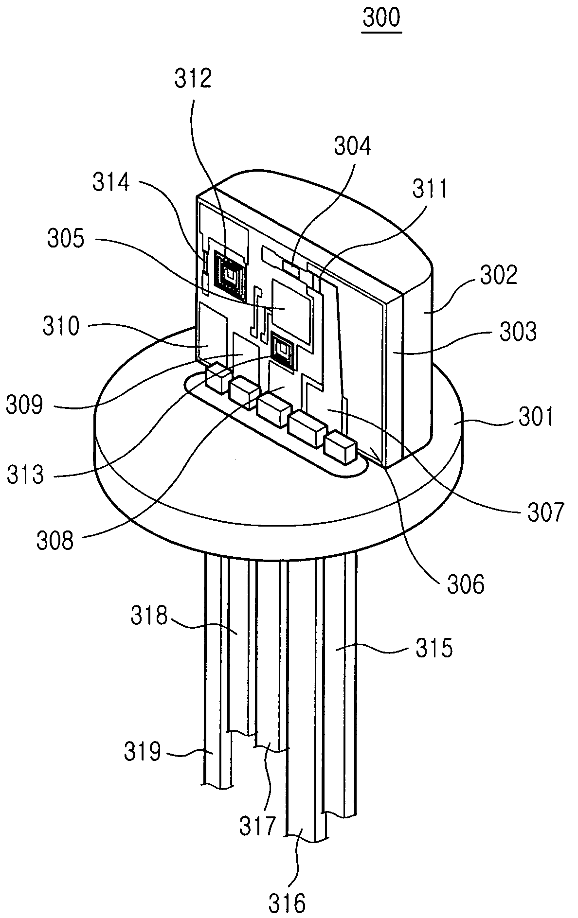
[0026]FIG. 3 illustrates a TO-can type optical module according to an aspect of the present invention. In particular, attention is directed to the structure of a sub-mount for a DML (Direct Modulated Laser) driver or cathode driven type.

[0027]Referring to FIG. 3, a TO-can type optical module 300 according to the present invention comprises a stem 301, a heat sink 302, a sub-mount 303, an LD 304, a PD 305, and a plurality of leads 315 to 319. Further included is CPW composed of 306, 307 and 308, an anode line 309 for the PD 305, a DC line 310, a matching resistor 311, first and second spiral inductors 312 a...


PUM


Abstract

A transistor-outline TO-can type optical module includes a stem, a sub-mount arranged in the stem and a laser diode (LD) is mounted in the sub-mount. A photo diode (PD), which has an inclined light incident surface, converts light emitted from the LD to current. A plurality of leads is extended through the stem while electrically being connected to the sub-mount. The inclined light incident surface of the PD permits that sufficient monitoring of photocurrent can be obtained and a p-side up bonding of a p-type electrode is allowed. Thus, the SMSR of the LOB is increased. A bias-tee is built in the TO-can to reduce heat caused by DC current and to increase opto-electric efficiency while suppressing an increase in the temperature of an LD chip.

Description

CLAIM FOR PRIORITY[0001]This application claims priority under 35 U.S.C. § 119 to an application entitled “TO-Can Type Optical Module,” filed in the Korean Intellectual Property Office on Nov. 14, 2003 and assigned Serial No. 2003-80505, the contents of which are incorporated herein by reference.BACKGROUND OF THE INVENTION[0002]1. Field of the Invention[0003]The present invention relates generally to an optical module. More particularly, the present invention relates to a TO-can (Transistor-Outline-can) type optical module.[0004]2. Description of the Related Art[0005]An optical module is an essential part of any system used for optical transmission. Owing to the recent rapid growth of the information industry, there are increasing proportions of information transmission traveling over an optical communication network, as well as increased demand for fast transmission and transmission of a large volume of information. The optical module must be designed to support fast and large-volu...

Claims


Application Information

Patent Timeline
Patent Type & Authority Patents(United States)
IPC IPC(8): G02B6/12G02B6/00G02B6/34G02B6/42G02B6/36H01S5/02H01S5/022H01S5/024H01S5/026H01S5/042H01S5/062H01S5/0683H04B10/00
CPCH01S5/02212H01S5/0071H01S5/02248H01S5/0683H01S5/0427H01S5/06226H01S5/02476H01S5/02325G02B6/42
Inventor KEH, YONG-CHANPARK, MUN-KUESHIN, DOO-SIKKIM, YU-SIK
Owner SAMSUNG ELECTRONICS CO LTD
Why Eureka
Try Eureka