Selective growth of ZnO nanostructure using a patterned ALD ZnO seed layer

a technology of zno nanostructure and seed layer, which is applied in the direction of single crystal growth, polycrystalline material growth, chemistry apparatus and processes, etc., can solve the problems of difficult subtractive patterning, difficult to etch metals used as catalysts for nanostructure growth, and inability to scatter particles onto substrates in ultra-clean environments used for microelectronic fabrication

Inactive Publication Date: 2007-12-04
SHARP KK
View PDF2 Cites 50 Cited by
  • Summary
  • Abstract
  • Description
  • Claims
  • Application Information

AI Technical Summary

Problems solved by technology

Nevertheless, dispersing particles onto a substrate in the ultra clean environments used for microelectronic fabrication is not desirable.
Additionally, the metals used as catalysts for nanostructure growth are typically difficult to etch and, consequently, are difficult to subtractively pattern.
Moreover, the metals used as catalysts are typically difficult to chemical mechanical polish (CMP).
Accordingly, nanostructure catalyst materials are typically difficult to pattern via conventional microelectronic processes.
Further, contamination from using a metal catalyst is also a concern because an eventual goal is to integrate nanostructures into a Si CMOS process and metal-catalyst contamination is potentially deleterious to Si CMOS devices.

Method used


Image

  • Selective growth of ZnO nanostructure using a patterned ALD ZnO seed layer
  • Selective growth of ZnO nanostructure using a patterned ALD ZnO seed layer
  • Selective growth of ZnO nanostructure using a patterned ALD ZnO seed layer

Examples


exemplary embodiment 100

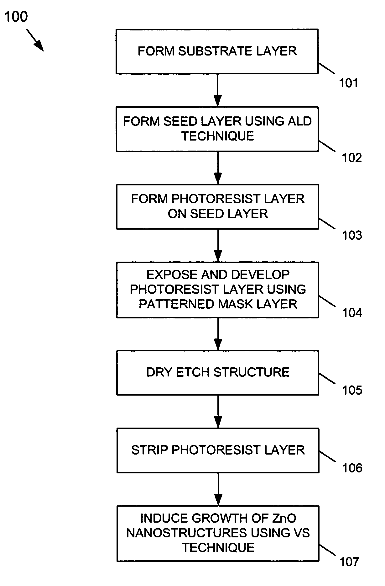
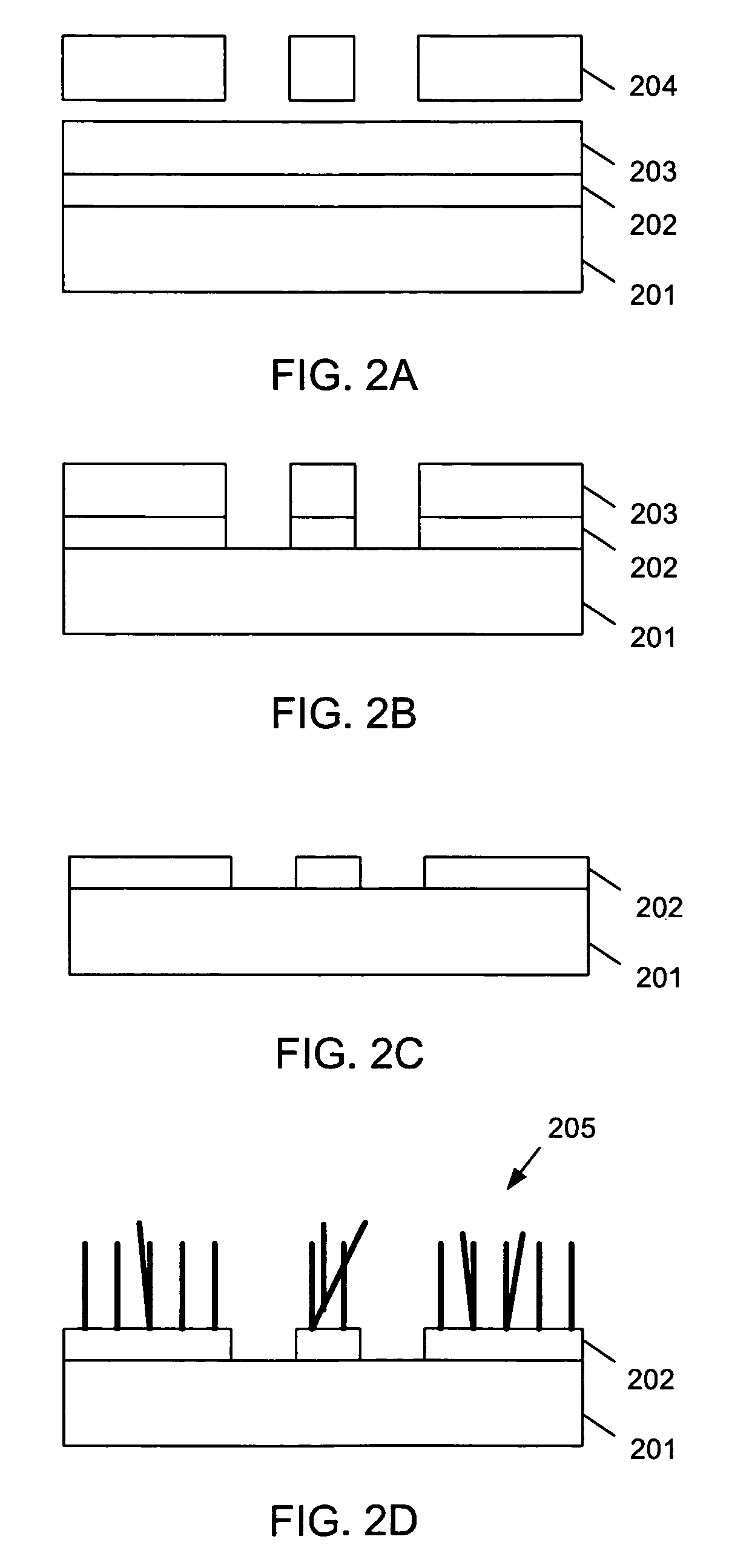
[0018]FIG. 1 depicts a flowchart for a first exemplary embodiment 100 of a technique for selectively forming ZnO nanostructures according to the present invention. FIGS. 2A-2D depict a sequence of cross-sectional views of a substrate and ZnO nanostructures that are formed by the first exemplary embodiment of a technique for selectively forming ZnO nanostructures according to the present invention. At step 101 in FIG. 1, a clean Si 100, or Si 111 starting wafer is used as a substrate layer 201 (FIG. 2A). At step 102, a thin seed layer 202 of polycrystalline ZnO is deposited on the surface of substrate layer 201 using Atomic Layer Deposition (ALD) (FIG. 2A). For ALD, precursors are pulsed alternately into the deposition chamber and are separated by purges. Reactions take place on the substrate surface and are self-limiting. Film thickness is controlled by the number of precursor pulse / purge cycles. The self-limiting nature of the process allows for uniformity and excellent conformalit...

exemplary embodiment 300

[0023]FIG. 3 depicts a flowchart for a second exemplary embodiment 300 of a technique for selectively forming ZnO nanostructures according to the present invention. FIGS. 4A and 4B depict a sequence of cross-sectional views of a substrate and ZnO nanostructures that are formed by the second exemplary embodiment of a technique for selectively forming ZnO nanostructures according to the present invention. At step 301 in FIG. 3, a clean Si 100 or Si 111 starting wafer is used as a substrate layer 401 (FIG. 4A). At step 302, a thin seed layer 402 of polycrystalline ZnO is deposited on the surface of substrate layer 401 using a spin-on technique (FIG. 4A). In one exemplary embodiment, layer 402 is formed by a Metal Organic Deposition (MOD) technique using zinc acetate dehydrate in 2-methoxyethanol and ethanolamine to form MOD ZnO that is about 80 nm thick. Any thickness of MOD ZnO for seed layer 402 could be used. Alternatively, ZnO layer 402 could be deposited using other methods, such ...


PUM

PropertyMeasurementUnit
thickaaaaaaaaaa
temperatureaaaaaaaaaa

Abstract

Patterned zinc-oxide nanostructures are grown without using a metal catalyst by forming a seed layer of polycrystalline zinc oxide on a surface of a substrate. The seed layer can be formed by an atomic layer deposition technique. The seed layer is patterned, such as by etching, and growth of at least one zinc-oxide nanostructure is induced substantially over the patterned seed layer by, for example, exposing the patterned seed layer to zinc vapor in the presence of a trace amount of oxygen. The seed layer can alternatively be formed by using a spin-on technique, such as a metal organic deposition technique, a spray pyrolisis technique, an RF sputtering technique or by oxidation of a zinc thin film layer formed on the substrate.

Description

BACKGROUND OF THE INVENTION[0001]1. Field of the Invention[0002]The present invention relates to nanotechnology and / or microelectronics. In particular, the present invention relates a method for forming zinc-oxide (ZnO) nanostructures on a silicon (Si) substrate.[0003]2. Description of the Related Art[0004]Nanostructured materials, such as nanowires, nanorods, nanofibers, whiskers, etc., exhibit interesting optical and electronic properties and have been demonstrated for many applications, such as chemical and bio sensors and detectors, LEDs, transistors, lasers, field emitters, etc. See, for example, P. Yang et al., “Controlled growth of ZnO nanowires and their optical properties,” Adv. Func. Mat. 12(5), 323 (2002) and C. M. Lieber, “Nanoscale science and technology: Building a big future from small things,” MRS Bulletin, pp. 486-491, (July 2003). Zinc oxide (ZnO), in particular, exhibits many interesting properties for nanostructures that could be useful for solid-state optoelectr...

Claims


Application Information

Patent Timeline
Patent Type & Authority Patents(United States)
IPC IPC(8): C30B25/04
CPCC30B25/02C30B29/605C30B29/16
Inventor CONLEY, JR., JOHN F.STECKER, LISA H.
Owner SHARP KK
Why Eureka
Try Eureka