Ferroelectric memory with wide operating voltage and multi-bit storage per cell

a ferroelectric memory and operating voltage technology, applied in the field of semiconductor devices, can solve the problems of large integration, difficult access to ferroelectric capacitors in cross-point arrays without, and disturbance of the state of capacitors, so as to avoid the increase of power requirements, reduce the effective area required for memory storage, and avoid higher voltage problems

Inactive Publication Date: 2007-12-04
TEXAS INSTR INC
View PDF21 Cites 22 Cited by
  • Summary
  • Abstract
  • Description
  • Claims
  • Application Information

AI Technical Summary

Benefits of technology

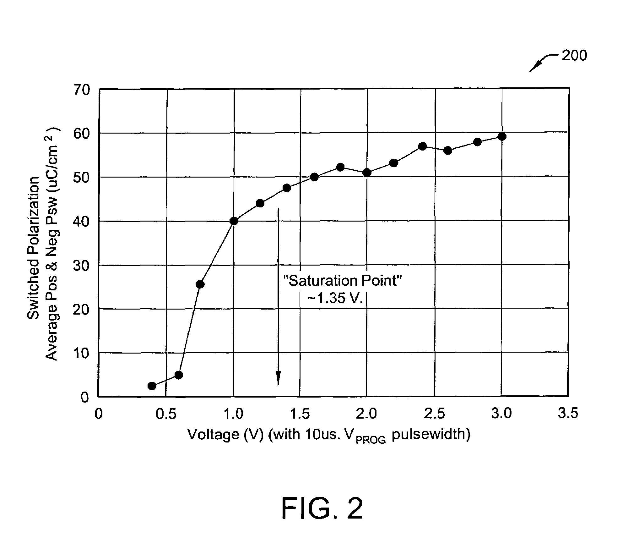
[0018]Optionally, in another aspect of the invention, a refresh circuit may be added to initiate a refresh operation comprising a restore (read and write) memory operation of the memory cell after a predetermined time period, wherein one of the plurality of program voltages and the reference voltage is used in the refresh operation, thereby periodically refreshing the memory cell data. By refreshing the memory cell data periodically, polarization charge levels which may be below the polarization saturation level of the FeCap are maintained at levels without a loss of data.
[0019]Thus, the invention may be employed to reduce the effective area required for memory storage, while avoiding the increased power requirements, and higher voltage problems experienced in some conventional designs. Moreover, the invention may be employed in memory structures enabling low voltage operation.
[0021]In another optional aspect of the invention, a refresh circuit may be added to initiate a refresh operation comprising a restore memory operation of the memory cell after a predetermined time period, wherein the program pulse and one of the plurality of reference voltages are used in the refresh operation, thereby periodically refreshing the polarization charge levels to original levels to avoid loss of data.

Problems solved by technology

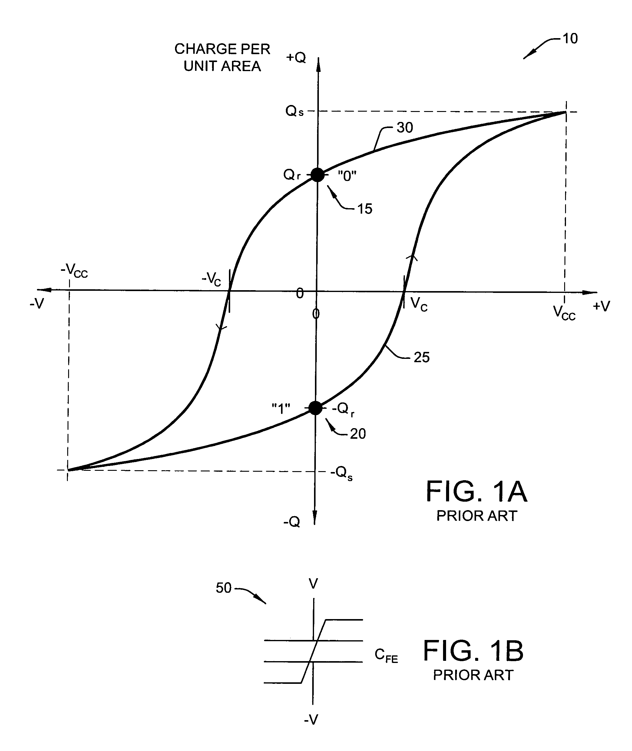
This reflects a partial switching of electric domains in a ferroelectric capacitor, and further implies that even a voltage level that is half of Vcc can disturb the state of the capacitor.
As a result, it is difficult to access a ferroelectric capacitor in a cross-point array without disturbing the capacitors on the same row or column.
Additionally, future products may require integration of large amounts of on-chip (embedded) memory.
However, few memory structures allow low voltage operation.
DRAM typically has a high power consumption, which makes DRAM fairly incompatible with the increasing demand for low power applications.
Attempts to scale the dielectric layer of Flash memory have proven to be difficult or impossible to scale due to degradation of the coupling ratio.
Although Flash memories are available with “two bits per cell” allowing a 2× density increase with some penalty of increased sensing circuitry area, Flash also requires high voltages for the program and erase memory operations.
As indicated, these memory technologies are not perfect and result in only marginal improvement, and may also be difficult to implement, particularly while scaling down the technologies and the operating voltage in memory devices.

Method used


Image

  • Ferroelectric memory with wide operating voltage and multi-bit storage per cell
  • Ferroelectric memory with wide operating voltage and multi-bit storage per cell
  • Ferroelectric memory with wide operating voltage and multi-bit storage per cell

Examples


Embodiment Construction

[0052]The present invention will now be described with reference to the attached drawings, wherein like reference numerals are used to refer to like elements throughout. The invention relates to memory apparatus and methodologies, which may be employed in write and read operations of a multi-level FeRAM memory device. One or more exemplary implementations of the various aspects of the invention are hereinafter illustrated and described in the context of ferroelectric memory devices comprising single transistor, single ferroelectric capacitor (1T1C) memory cells organized in folded bit line architectures.

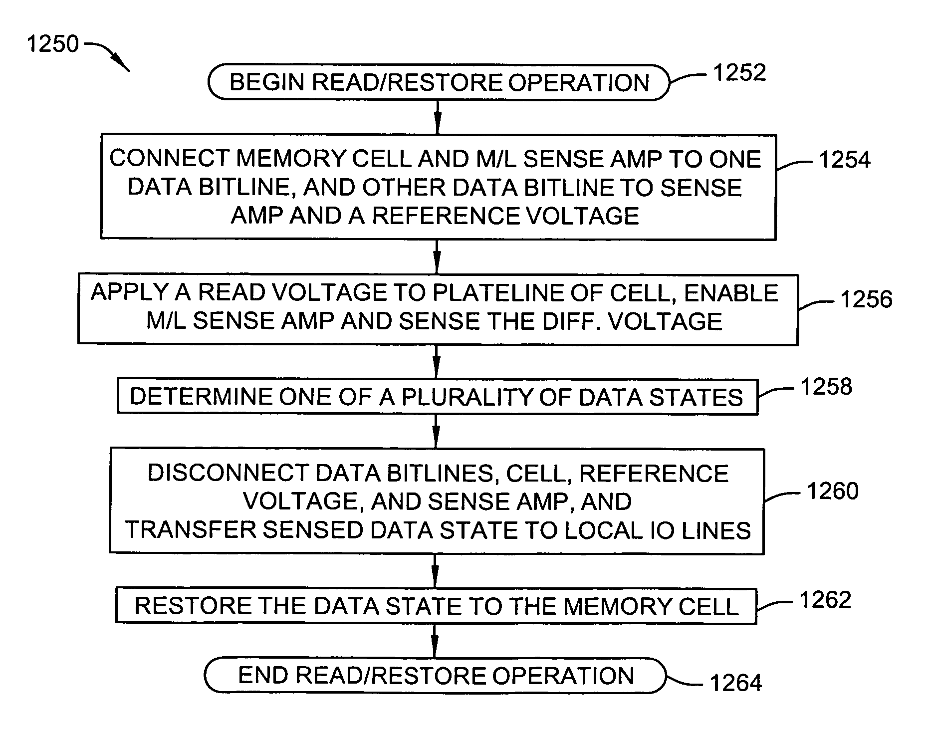
[0053]In the above exemplary architecture, a program pulse is coupled with the memory cell during a write operation to store data in the FeCap as one of a plurality of switched and non-switched polarization charge levels (polarization charge levels, or magnitudes). During a read operation, a multi-level sense amp circuit is coupled to the first and second data bit lines with the ferr...


PUM


Abstract

Apparatus and methods are described for a multi-level FeRAM memory device. Using write and read circuits associated with the memory device, multiple data states may be written to and read from the ferroelectric memory device which are associated with a single polarization direction, thereby allowing for a single cell to contain more than one bit of data.

Description

RELATED APPLICATION[0001]This application divisional of Ser. No. 10 / 260,467 filed Sep. 30, 2002, now U.S. Pat. No. 6,856,534 which is entitled “Ferroelectric Memory with Wide Operating Voltage and Multi-Bit Storage Per Cell”.FIELD OF INVENTION[0002]The present invention relates generally to semiconductor devices and more particularly to apparatus and methods for multiple bit data storage and retrieval in ferroelectric memory cells, while operating the cells over a wide voltage range in memory devices.BACKGROUND OF THE INVENTION[0003]Ferroelectric memory devices, and other types of semiconductor memories, are used for storing data and / or program code in personal computer systems, embedded processor-based systems, and the like. Ferroelectric memories are commonly organized in single-transistor, single-capacitor (1T1C) or two-transistor, two-capacitor (2T2C) configurations, in which data is read from or written to the device using address signals and various other control signals. The ...

Claims


Application Information

Patent Timeline
Patent Type & Authority Patents(United States)
IPC IPC(8): G11C11/22G11C11/56H01L21/8246H01L27/105
CPCG11C11/22G11C11/5657G11C2211/5641
Inventor RODRIGUEZ, JOHN ANTHONYUDAYAKUMAR, KEZHAKKEDATH R.
Owner TEXAS INSTR INC
Why Eureka
Try Eureka