Localized synthesis and self-assembly of nanostructures

a nanostructure and localization technology, applied in the field of nano-to-micro integration, can solve the problems of affecting the application of nanostructures, affecting the stability of nanostructures, so as to prevent time-consuming post-growth manipulation and expensive, controlled and accurate positioning, the effect of hot spo

Active Publication Date: 2007-12-25
RGT UNIV OF CALIFORNIA
View PDF5 Cites 34 Cited by
  • Summary
  • Abstract
  • Description
  • Claims
  • Application Information

AI Technical Summary

Benefits of technology

[0010]The approach of the present invention is based on localized resistive heating of suspended microstructures in a room temperature chamber to activate silicon nanowire or carbon nanotube synthesis via the vapor-liquid-solid (VLS) growth mechanism. By employing localized heating in the growth of the nanowires or nanotubes, the structures can be synthesized on a device in a room temperature chamber without the device being subjected to overall heating. The method is localized and selective, and provides for a suspended microstructure to achieve the thermal requirement for vapor deposition synthesis, while the remainder of the chip or substrate remains at room temperature. Accordingly, sensitive processed devices are not subjected to damaging heat during fabrication of the nanotubes and nanowires.
[0011]Furthermore, by employing electric field assisted self-assembly techniques according to the present invention, it is not necessary to grow the nanotubes and nanowires and separately connect them to a device. Instead, the present invention provides for self-assembly of nanostructures such as nanotubes and nanowires on the devices, such as integrated circuits, themselves, thus providing for nano- to micro-integration.
[0013]By way of example, and not of limitation, in one embodiment of the invention a microscale conductive element is fabricated using standard bulk and surface micromachining techniques. An appropriate catalyst layer is then deposited atop the microstructure, with a thickness of several nanometers. A current is passed through the microstructure which causes it to resistively heat. By controlling the current and voltage applied to the microstructure, a hot spot can be controlled and accurately located in the microstructure. This hot spot then provides the energy necessary to instigate and sustain synthesis of the nanostructure of interest; The ambient environment during nanomaterial synthesis includes a room-temperature pressure-controlled vacuum chamber and room temperature, mass-flow-controlled precursor, active, and inert gasses. This allows for fabrication of integrated nanostructures in one localized region on or above a chip, while the bulk of the microchip remains at room temperature.
[0014]Therefore, another aspect of the invention is to integrate nanomaterials with standard microelectronics and / or MEMS devices. This direct integration is a key step for nanomaterial implementation, as it implicitly precludes time-consuming post-growth manipulation and expensive e-beam lithography. Such direct integration, or self-assembly, is facilitated by application of an electric field to the region of nanostructure synthesis. Nanostructure growth follows the direction of the electric field lines and, therefore, the direction of nanostructure growth can be controlled. The nanostructure is then synthesized from the growth structure as described above to a secondary structure which the nanostructure contacts and bonds thereto.
[0017]In another mode of the current aspect, generating localized microresistive heating comprises passing current through a resistive element to provide localized heating to initiate and sustain nanostructure growth. Generally, a catalyst is deposed on the resistive element prior to heating. The catalyst facilitates a VLS (vapor-liquid-solid) synthesis process upon heating of the resistive element to generate nanostructure growth.
[0019]Another aspect of the invention is a method for synthesizing a nanostructure, comprising the steps of providing a resistive microstructure, passing a current through the microstructure to cause it to resistively heat in a room-temperature environment, and controlling the temperature of a location on the microstructure by controlling the current and voltage applied to the microstructure. The controlled location on the microstructure provides the energy necessary to instigate and sustain synthesis of the nanostructure of interest.

Problems solved by technology

However, a significant obstacle in the application of these nanostructures has been the difficulty in handling, maneuvering, and integrating them with microelectronics to form a complete system.
Current synthesis processes for silicon nanowires and carbon nanotubes require high temperature furnaces that could damage pre-existing microelectronics.

Method used


Image

  • Localized synthesis and self-assembly of nanostructures
  • Localized synthesis and self-assembly of nanostructures
  • Localized synthesis and self-assembly of nanostructures

Examples


example 1

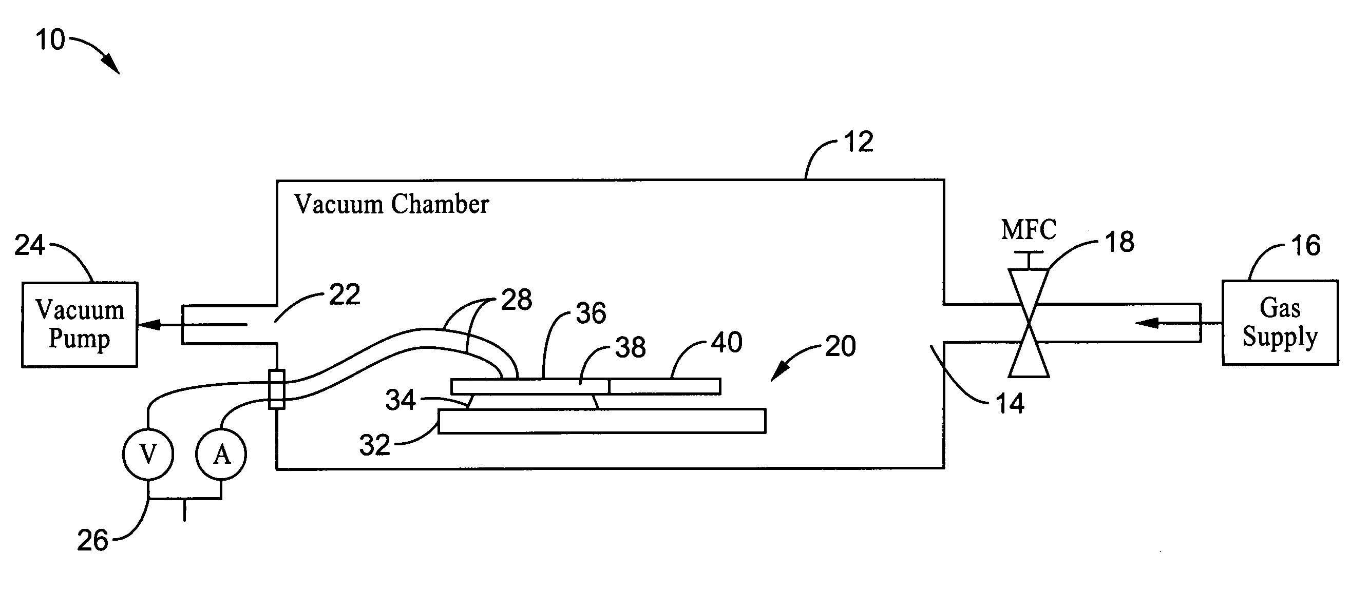
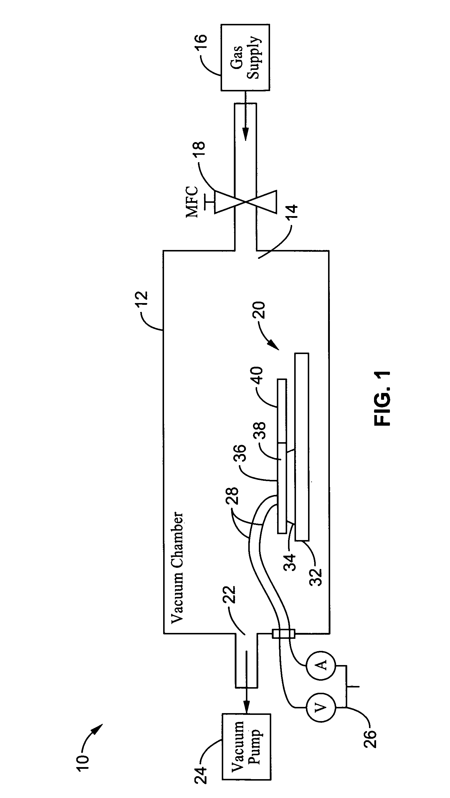
[0066]Two types of suspended microelectromechanical systems (MEMS) structures were fabricated to serve as localized microresistive heaters for the synthesis processes: (i) polysilicon microstructures using a standard surface micromachining process, and (ii) bulk-etched single crystal silicon (SCS) microstructures based on a silicon on insulator (SOI) wafer. The synthesis processes were carried out in a growth chamber 10 having a vacuum chamber 12 at room temperature as shown schematically in FIG. 1. A treatment gas is supplied to the vacuum chamber 12 at inlet 14 via gas supply 16, and is controlled by mass flow controller 18. Microstructure 20 is positioned inside the vacuum chamber 12 and is connected to power supply 26 via leads 28. Vacuum pump 24 draws gas out of the chamber via outlet 22.

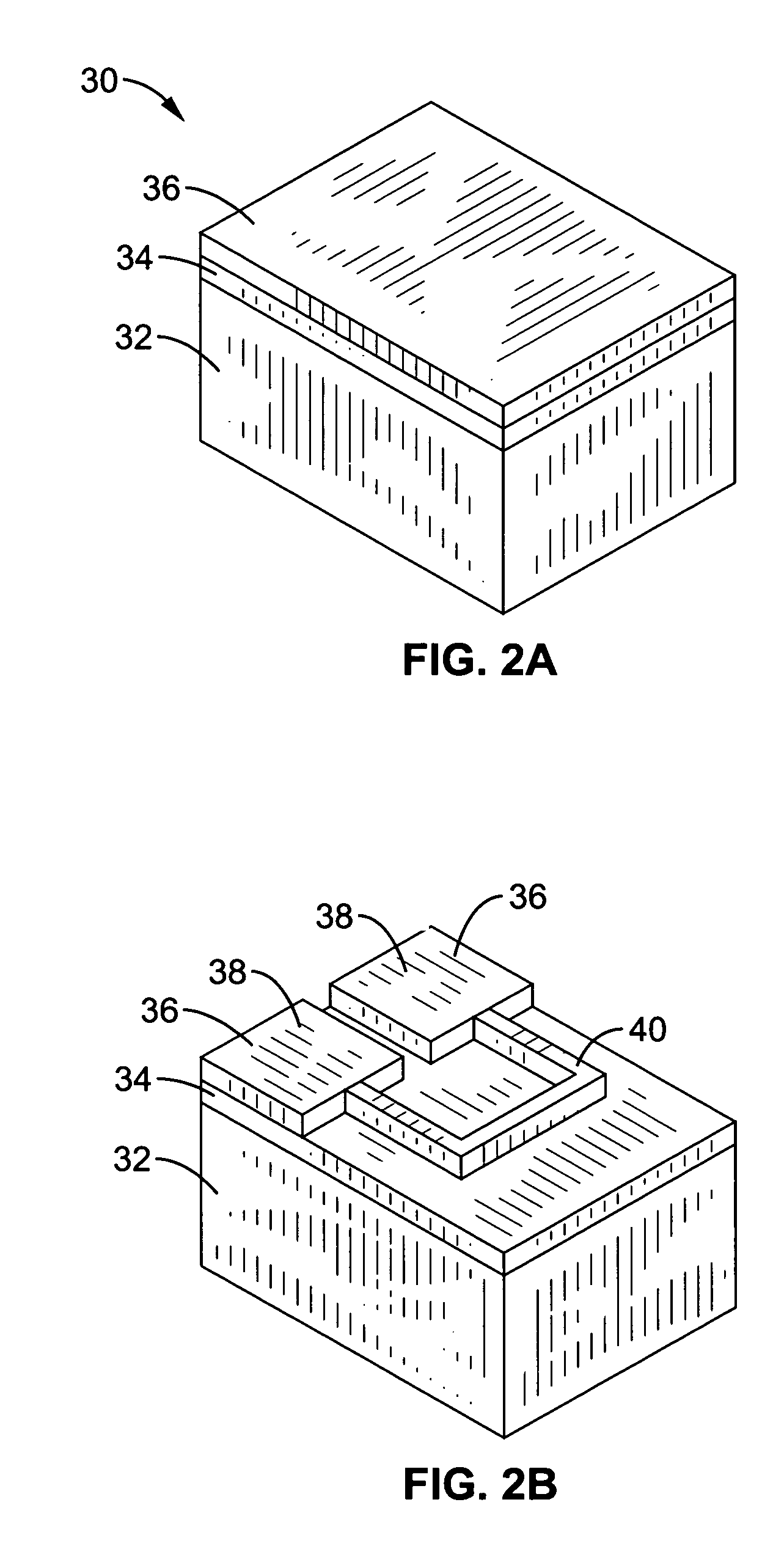
[0067]FIGS. 2A through 2G illustrate the fabrication of microstructure 20 and use in growth chamber 10 for generation of nanostructures. FIG. 2A illustrates an initial three-layer wafer 30 used...

example 2

[0087]For nanotube synthesis, the same method and phenomena described above with respect to nanowire synthesis are employed. In this embodiment, a thin metal layer 42 was evaporated over the entire chip to serve as a the catalyst for growth. A mixture of approximately 5 nm nickel, iron, or Ni—Fe (80% to 20% by weight) was used as the catalyst, with higher growth rates occurring when iron was present (e.g., see FIG. 2D). After wirebonding for electrical connectivity, the microstructures were placed into a room temperature vacuum chamber (e.g., see, FIG. 2E). The organic vapor phase, acetylene (C2H2), was introduced at 245 mTorr to supply carbon and the microstructure was heated to initiate nanotube synthesis (e.g., see FIG. 2E). With the acetylene pressure constant at 245 mTorr, growth occurred at 0.25 μm / min at optimal temperature locations. Note that growth rate may also depend on the pressure. Note also that carbon nanotube (CNT) growth requires higher temperatures for the synthes...

example 3

[0098]We also demonstrated that orientation of nanotubes 76 is a function of the electric field E as shown in FIGS. 13A-B. The bottom right side 80 of this “U-shaped” microstructure 40 was taken to approximately 7V, while the bottom left side 82 was grounded, yielding an electric field of approximately 0.12 V / μm in the region where the longest growth occurred. This region is further detailed in expanded view of FIG. 13B which shows the CNT from outside the microstructure 40 curving with the electric field E. This electric field is weaker than desirable for oriented CNT growth, but shows that the electric field due to the synthesis process alone can be used to orient the tubes. The addition of additional electric field, by increasing the potential difference between nearby microstructures, will enhance this effect.

[0099]It will be appreciated that assembly is probably the most difficult task in any nanostructure integration process. To facilitate assembly, the present invention uses ...


PUM

PropertyMeasurementUnit
diameteraaaaaaaaaa
diameteraaaaaaaaaa
diametersaaaaaaaaaa

Abstract

Systems and methods for local synthesis of silicon nanowires and carbon nanotubes, as well as electric field assisted self-assembly of silicon nanowires and carbon nanotubes, are described. By employing localized heating in the growth of the nanowires or nanotubes, the structures can be synthesized on a device in a room temperature chamber without the device being subjected to overall heating. The method is localized and selective, and provides for a suspended microstructure to achieve the thermal requirement for vapor deposition synthesis, while the remainder of the chip or substrate remains at room temperature. Furthermore, by employing electric field assisted self-assembly techniques according to the present invention, it is not necessary to grow the nanotubes and nanowires and separately connect them to a device. Instead, the present invention provides for self-assembly of the nanotubes and nanowires on the devices themselves, thus providing for nano-to micro-integration.

Description

CROSS-REFERENCE TO RELATED APPLICATIONS[0001]This application claims priority from U.S. provisional application Ser. No. 60 / 533,778 filed on Dec. 30, 2003, incorporated herein by reference in its entirety.STATEMENT REGARDING FEDERALLY SPONSORED RESEARCH OR DEVELOPMENT[0002]Not applicable.INCORPORATION-BY-REFERENCE OF MATERIAL SUBMITTED ON A COMPACT DISC[0003]Not ApplicableNOTICE OF MATERIAL SUBJECT TO COPYRIGHT PROTECTION[0004]A portion of the material in this patent document is subject to copyright protection under the copyright laws of the United States and of other countries. The owner of the copyright rights has no objection to the facsimile reproduction by anyone of the patent document or the patent disclosure, as it appears in the United States Patent and Trademark Office publicly available file or records, but otherwise reserves all copyright rights whatsoever. The copyright owner does not hereby waive any of its rights to have this patent document maintained in secrecy, incl...

Claims


Application Information

Patent Timeline
Patent Type & Authority Patents(United States)
IPC IPC(8): C30B19/12C01B31/02C01B33/02C23C16/02C23C16/24C23C16/26C23C16/44H01L21/20H01L29/00H01L51/00
CPCB82Y10/00B82Y40/00C01B31/0233C01B33/02C23C16/0281C23C16/24C23C16/26H01L21/02381H01L21/02532H01L21/02603H01L21/02606H01L21/0262H01L21/02636H01L21/02645H01L21/02653H01L51/0002B82Y30/00H01L51/0052C01B2202/34C01B2202/36H01L51/0048C01B32/162H10K71/10H10K85/221H10K85/615
Inventor LIN, LIWEIENGLANDER, ONGICHRISTENSEN, DANE
Owner RGT UNIV OF CALIFORNIA
Why Eureka
Try Eureka