Multilayer wiring board, base for multilayer wiring board, printed wiring board and its manufacturing method

a multi-layer wiring and wiring board technology, applied in the direction of printed element electric connection formation, semiconductor/solid-state device details, instruments, etc., can solve the problems of reducing the flexibility of circuit layout design, unable to mount a chip, and unable to meet the demands of high-density packaging, etc., to achieve the effect of increasing the contact area

Inactive Publication Date: 2007-12-25
FUJIKURA LTD
View PDF3 Cites 43 Cited by
  • Summary
  • Abstract
  • Description
  • Claims
  • Application Information

AI Technical Summary

Benefits of technology

[0027]In accordance with this multilayer wiring board assembly component, the electrical connection between a conductive layer and a conductive resin composition is made by the use of the differential bore diameter of a through hole between the insulating substrate component and the conductive layer portion thereof, and therefore it is possible to solve the respective problems originating from the requirement of securing the contact area between the conductive layer and the portion of the conductive resin composition located above the conductive layer.
[0112]On the other hand, in accordance with the printed circuit board of this invention, where connection is made by a solder bump, the solder bump is melted and bonded to the metallic layer in a form conforming to the concave surface of the metallic layer and therefore the deformation of the locally deformed portion in the boundary surface between the solder bump and the substrate electrode is alleviated as compared with that in accordance with the prior art technique. Accordingly, the concentration of stress to the locally deformed portion is alleviated to improve the connection reliability between the chip and the substrate. Also, the solder bump does not contact with the conductive paste filling the via hole but contacts with only the metallic layer therefore, the solder wetting becomes uniform and improves. In the case of a gold bump, a self alignment effect appears while the bump is aligned with the location by means of the concave surface of the substrate electrode.

Problems solved by technology

In the case of a multilayered FPC with through halls, it is impossible to mount a chip on a through hall to decrease the flexibility of designing circuit layouts due to the restriction on the location of the interlayer interconnection.
Therefore, there is a definite ceiling to the implementation density, and it is impossible to meet the demands for high density packaging.
However, if this technique is applied to the structure as proposed in Japanese Patent Application No. 2001-85224, a portion of the conductive resin composition 5 (the head shaped projection 5A) located above the copper foil 2 is excessively squashed and extended as illustrated in FIG. 4 under the lamination pressure P during multilayer lamination so that it is difficult to make the dimensions of the respective head shaped projection 5A even, as seen from the surface of the substrate, therefore, in addition to this, a short-circuit would be formed.
In the case of the flip chip implementation that makes use of solder bumps for making connection, there is a problem in that the chip may be disconnected from the substrate due to stress generated at the connection interface between the substrate and the chip by mechanical shock or heat as generated by the operation of the chip.
This causes the bump connection method to lose it's advantage over the wire bonding technique.
Namely, defects due to contact between different materials are concentrated at the boundary surface therebetween at which a mechanically fragile composition layer of tin and copper is segregated and which is estimated to be the starting point of destruction.
In the case of the technique that makes use of solder bumps, while a self alignment effect is known as automatic alignment of a chip with a substrate by solder wetting on the electrode during the reflow process for melting the solder, the self alignment effect can not be expected in the case of gold bumps so it is difficult to align a chip to a substrate.

Method used


Image

  • Multilayer wiring board, base for multilayer wiring board, printed wiring board and its manufacturing method
  • Multilayer wiring board, base for multilayer wiring board, printed wiring board and its manufacturing method
  • Multilayer wiring board, base for multilayer wiring board, printed wiring board and its manufacturing method

Examples


first embodiment

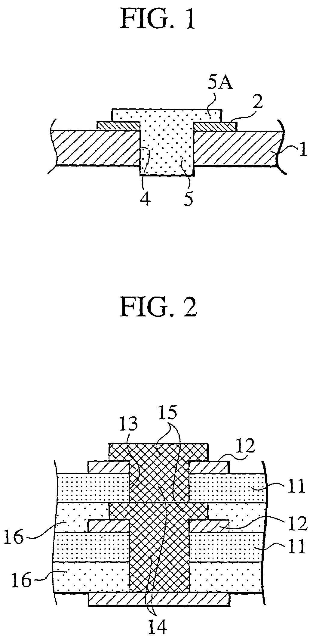
[0197]FIG. 7 and FIG. 8 show the basic configuration of multilayer wiring board assembly components in accordance with the present invention.

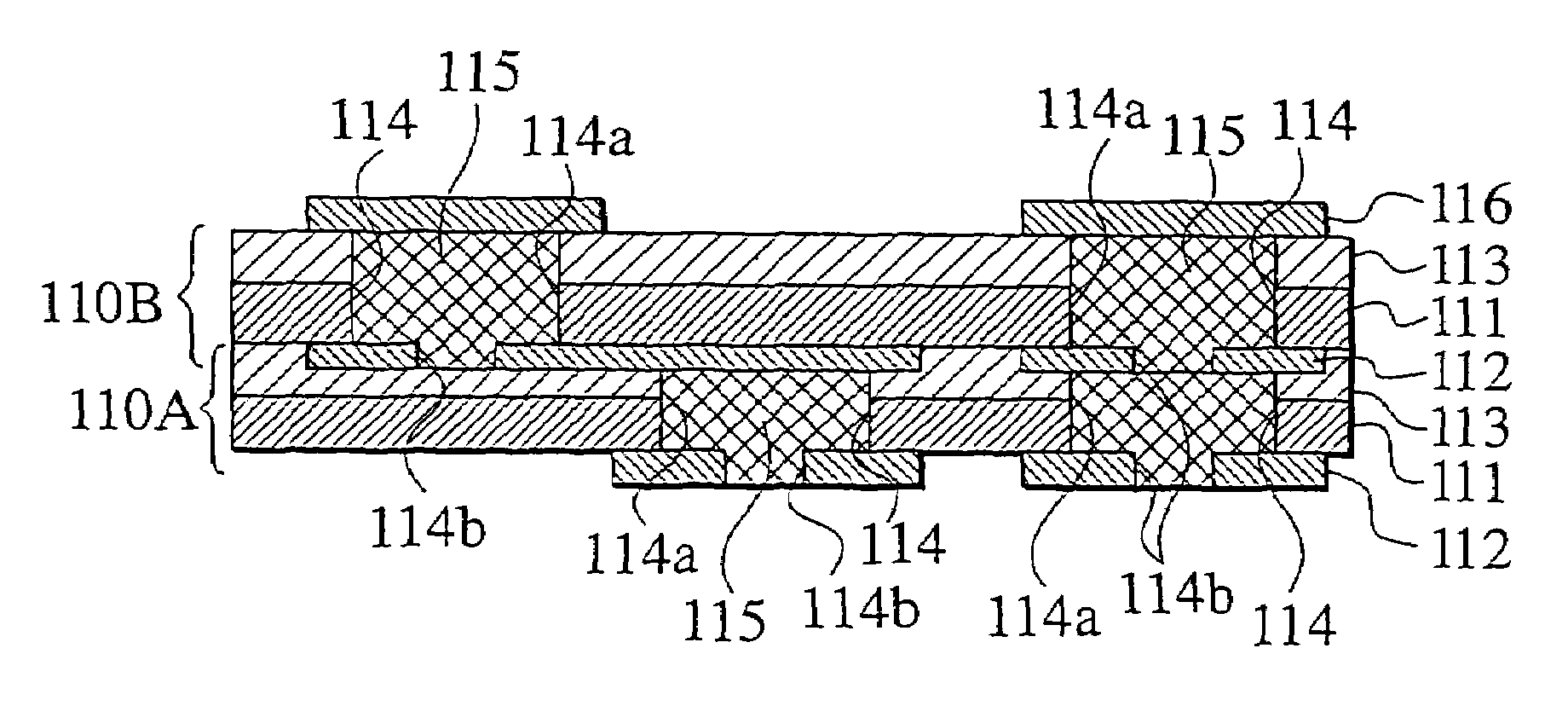
[0198]The multilayer wiring board assembly component as illustrated in FIG. 7 is composed of an insulating resin layer 111 as an insulating substrate component which is provided with a conductive layer 112 made of copper foil and the like as an electrode pattern on one surface of the insulating resin layer 111 and an adhesive layer 113 for interlayer connection on the other surface respectively with a through hole 114 formed that passes through the adhesive layer 113, the insulating resin layer 111 and the conductive layer 112. The through hole 114 is filled with a conductive resin composition 115 in order to form an IVH (via hole).

[0199]In the case of an FPC, the insulating resin layer 111 is composed of a flexible resin film such as a polyimide film, a polyester film or the like made of a wholly aromatic polyimide (API) and the like in order ...

second embodiment

[0248]In what follows, the second embodiment in accordance with the present invention will be explained in detail with reference to the accompanied drawings.

[0249]FIG. 17 shows the basic configuration of a multilayer wiring board assembly component in accordance with the second embodiment of the present invention.

[0250]The multilayer wiring board assembly component as illustrated in FIG. 17 is composed of an insulating resin layer 211 as an insulating substrate component which is provided with a conductive layer 212 of a copper foil and the like as an electrode pattern on one surface of the insulating resin layer 211 and an adhesive layer 213 for interlayer connection on the other surface respectively with a through hole 214 formed passing through the adhesive layer 213, the insulating resin layer 211 and the conductive layer 212. The through hole 214 is filled with a conductive resin composition 215 in order to form an IVH (via hole).

[0251]In the case of an FPC, the insulating resi...

third embodiment

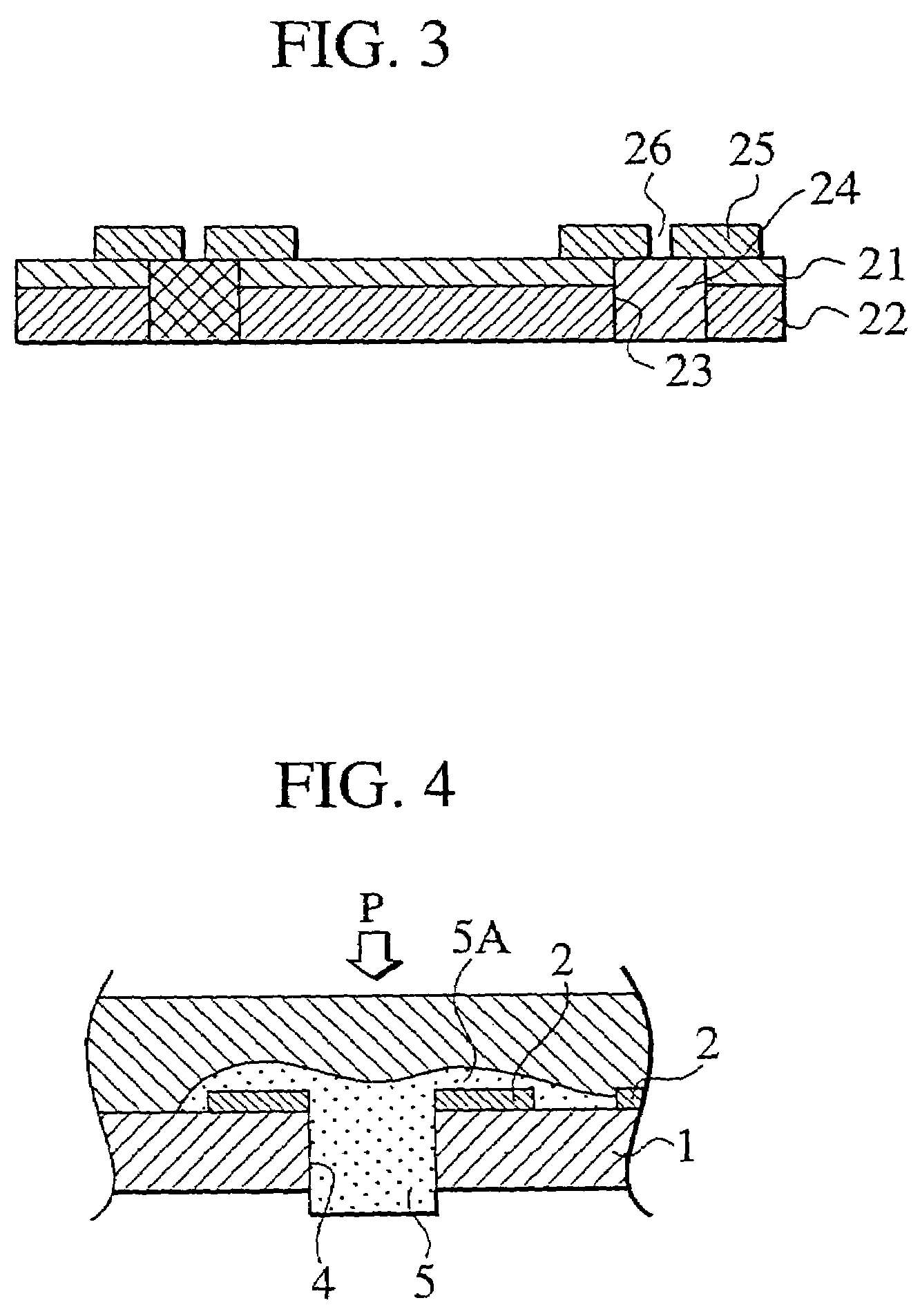
[0278]FIG. 22 shows the basic configuration of a multilayer wiring board assembly component in accordance with the present invention.

[0279]In the multilayer wiring board assembly component as illustrated in FIG. 22, the insulating resin layer 221 itself, as an insulating substrate component, has adhesivity for interlayer connection and is provided with a conductive layer 222 made of a copper foil and the like as an electrode pattern on one surface of the insulating resin layer 221 while the through hole 224 is opened through the insulating resin layer 221 and the conductive layer 222. The through hole 224 is filled with the conductive resin composition 225 in order to form an IVH (via hole).

[0280]In the case of an FPC, the insulating resin layer 221 having adhesivity is formed of a thermoplastic polyimide (TPI) or a thermoplastic polyimide to which a thermosetting property is given. In the case of the use of a thermoplastic polyimide film, taking into consideration the heat resistan...


PUM


Abstract

A multilayer wiring board assembly component comprises: an insulating substrate component (the insulating resin layer 111); a conductive layer 112 formed on one surface of said insulating substrate component 111 in the form of an electrode pattern; an adhesive layer 113 formed on the other surface of said insulating substrate component 111; and a conductive resin composition 115 with which is filled a through hole passing through said insulating substrate component 111, said adhesive layer and said conductive layer in order to make interlayer interconnection. The bore diameter of the conductive layer portion 114b of the through hole 114 is smaller than the bore diameter of the insulating resin layer portion and the adhesive layer portion 114a to establish electrical connection between the conductive resin composition 115 and the conductive layer 112 by the rare surface 112a of the conductive layer 112.

Description

TECHNICAL FIELD[0001]The present invention is related to a multilayer wiring board assembly (a multilayer printed circuit board), a multilayer wiring board assembly component, a printed circuit board and a manufacturing method thereof. Particularly, the present invention is related to a multilayer wiring board assembly, a multilayer wiring board assembly component and a manufacturing method thereof in which the multilayer wiring board assembly can be implemented with a high packing density by the flip chip mounting technique and so forth.[0002]Also, in particular, the present invention is related to a multilayer wiring board assembly, a multilayer wiring board assembly component and a manufacturing method thereof in which interlayer interconnection is established by the use of a conductive resin composition (conductive paste) with which a via hole is filled. Furthermore, the present invention is related to a printed circuit board for implementing a flip chip and the manufacturing me...

Claims


Application Information

Patent Timeline
Patent Type & Authority Patents(United States)
IPC IPC(8): H05K1/00H05K3/38H05K3/40H05K3/46
CPCH05K3/4069H05K3/4617H05K3/386H05K3/4652H05K2201/0195H05K2201/0394Y10T428/12181H05K2201/09827H05K2201/09863H05K2203/0191H05K2203/1453Y10T428/24917Y10T29/49165H05K2201/0969H05K3/40H05K3/46
Inventor ITO, SHOJINAKAO, OSAMUHIGUCHI, REIJIOKAMOTO, MASAHIRO
Owner FUJIKURA LTD
Why Eureka
Try Eureka