Chip-stacked semiconductor package and method for fabricating the same

a technology of semiconductor packages and chips, applied in semiconductor devices, semiconductor/solid-state device details, electrical devices, etc., can solve the problems of poor thermal conductivity, affecting the performance and lifetime of chips, and affecting the heat dissipation efficiency of chips, so as to facilitate the mass production of semiconductor packages and avoid excessive wear of cutting tools

Active Publication Date: 2008-01-01
SILICONWARE PRECISION IND CO LTD
View PDF14 Cites 23 Cited by
  • Summary
  • Abstract
  • Description
  • Claims
  • Application Information

AI Technical Summary

Benefits of technology

[0012]In light of the foregoing drawbacks in the conventional technology, an objective of the present invention is to provide a chip-stacked semiconductor package and a method for fabricating the same, which can effectively integrate a heat dissipating structure in the multi-chip semiconductor package to thereby improve the heat dissipating efficiency.
[0013]Another objective of the present invention is to provide a chip-stacked semiconductor package and a method for fabricating the same, which can effectively integrate a heat dissipating structure in the multi-chip semiconductor package, without having a concern of area limitation in a CSP structure.
[0014]Still another objective of the present invention is to provide a chip-stacked semiconductor package and a method for fabricating the same, which can improve the heat dissipating efficiency and electrical quality of the multi-chip semiconductor package.

Problems solved by technology

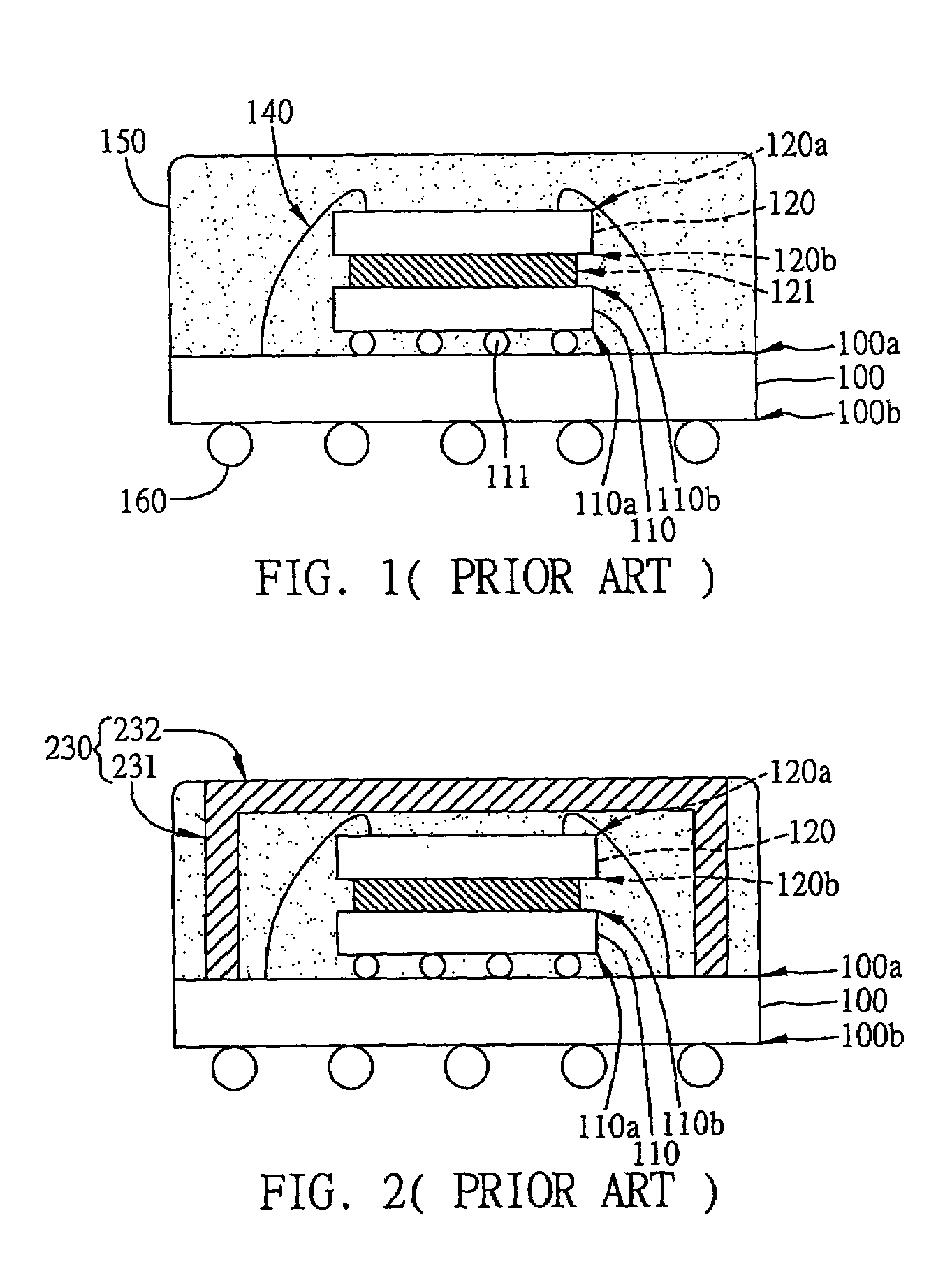
However, the foregoing stacked-type BGA chip package structure has a drawback that a large amount of heat is produced along with the operation of the highly integrated chips, and the encapsulant for encapsulating the chips is made of a poor thermally conductive resin material with a coefficient of thermal conductivity of only 0.8 w / m-k, thereby resulting in unsatisfactory heat dissipating efficiency and affecting the performances and lifetime of the chips.
However, in practical implementation, as the heat sink 230 of the package structure shown in FIG. 2 is not directly in contact with the non-active surfaces 110b, 120b of the two chips 110, 120, the heat produced by the chips 110, 120 must be transferred through the resin material with poor thermal conductivity to the heat sink 230, thereby not able to provide satisfactory heat dissipating efficiency.
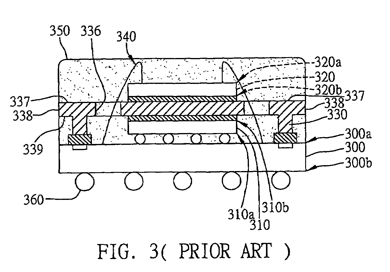
However in the CSP structure, since the substrate has a size nearly equal to the size of the chip and the area for bonding the conductive wires is limited to a portion between the chip attach area and edges of the substrate, there is no space on the substrate available for receiving a supporting portion of a heat sink.
Moreover, to accommodate the supporting portion of the heat sink on the substrate also causes a trouble in the manufacture of the substrate.
However, this arrangement requires corresponding modification of the substrate structure, and also easily causes slanting of the heat sink mounted on the solder balls due to difficulty in controlling the height of the solder balls.
The slanted heat sink may possibly come into contact with signal wires of the chip and thereby results in a short-circuiting problem.
This as a result leads to inconvenience in the fabrication processes, degraded reliability and increased costs.
And similarly, to accommodate the supporting portions (solder balls) for the heat sink on the substrate causes a trouble in the manufacture of the substrate.
Further in the foregoing semiconductor packages, the attachment between the heat sink and the chip needs to be precisely controlled to avoid slanting of the heat sink, such that a batch-type method cannot be used to attach heat sinks to chips.
That is, the heat sinks must be adhered to the corresponding chips one by one, thereby increasing the complexity and time of the overall packaging processes, which is undesirable for reducing the packaging costs and improving the packaging efficiency.

Method used


Image

  • Chip-stacked semiconductor package and method for fabricating the same
  • Chip-stacked semiconductor package and method for fabricating the same
  • Chip-stacked semiconductor package and method for fabricating the same

Examples


first embodiment

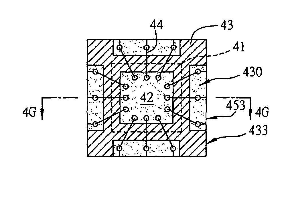
[0035]FIGS. 4A to 4H show steps of a method for fabricating chip-stacked semiconductor packages according to a first embodiment of the present invention.

[0036]Referring to FIGS. 4A and 4B, firstly, a chip carrier module plate such as a substrate module plate 40A is provided, which includes a plurality of chip carriers such as substrates 40 arranged in an array. Each of the substrates 40 has a first surface 401 and a second surface 402 opposed to the first surface 401. A plurality of first bond pads 403 and second bond pads 404 are formed on the first surface 401 of each of the substrates 40. The first bond pads 403 are located at a central portion of the first surface 401 of each of the substrates 40, such that a first chip 41 is attached and electrically connected to the first bond pads 403 of each of the substrates 40 in a flip-chip manner. The second bond pads 404 are located at a peripheral portion of the first surface 401 of each of the substrates 40 to subsequently allow a sec...

second embodiment

[0044]FIG. 6 is a cross-sectional view of a semiconductor package according to a second embodiment of the present invention. The semiconductor package in the second embodiment is fabricated by a method similar to that for the semiconductor package in the first embodiment, with a difference in that in the second embodiment, during a wire-bonding process for a second chip 52, a heat sink 53 serves as a ground plane such that the second chip 52 is electrically connected to the heat sink 53 via grounding wires 540 to thereby improve the electrical performance of the semiconductor package. In order for the heat sink 53 to provide electrical connection with the grounding wires (such as gold wires), silver is plated at positions on the heat sink 53 for connecting the grounding wires so as to improve the bondability between the heat sink 53 and the grounding wires.

third embodiment

[0045]FIG. 7 is a cross-sectional view of a semiconductor package according to a third embodiment of the present invention. The semiconductor package in the third embodiment is fabricated by a method similar to that for the semiconductor package in the first embodiment, with a difference in that a chip carrier used in the third embodiment is a LGA (Land Grid Array) substrate 60, such that a first chip 61 and a second chip 62 can be electrically connected to an external device through a plurality of metal contacts 60a provided on a bottom surface of the LGA substrate 60.


PUM


Abstract

A chip-stacked semiconductor package and a method for fabricating the same are proposed. A chip carrier module plate including a plurality of chip carriers, and a heat sink module plate including a plurality of heat sinks are provided, wherein a plurality of through holes are formed around each of the heat sinks. First chips, the heat sink module plate, and second chips are successively stacked on the chip carrier module plate, wherein the second chips are electrically connected to the chip carrier module plate by conductive wires penetrating the through holes of the heat sink module plate. After a molding process is completed, a singulation process can be performed to separate the chip carriers and the heat sinks, and thus individual semiconductor packages for integrating the heat sinks with the stacked chips are fabricated.

Description

FIELD OF THE INVENTION[0001]The present invention relates to chip-stacked semiconductor packages and methods for fabricating the same, and more particularly, to a chip-stacked semiconductor package for integrating a heat sink with stacked chips, and a method for fabricating the semiconductor package.BACKGROUND OF THE INVENTION[0002]The tremendous advancement of electronic industry leads electronic products to develop with multi-functionality and high performances to satisfy the packaging requirements such as high integration and miniaturization for semiconductor packages. In order to improve the performance and capacity of a single semiconductor package for use in a miniaturized electronic product with large capacity and high speed, the semiconductor package is conventionally made in the form of a MCM (multi chip module), which can reduce the overall volume and improve the electrical performance of the package and thus becomes a primary type of package in the industry. In the MCM st...

Claims


Application Information

Patent Timeline
Patent Type & Authority Patents(United States)
IPC IPC(8): H01L23/02
CPCH01L24/85H01L24/97H01L25/0657H01L25/50H01L24/45H01L2224/16225H01L2224/45144H01L2224/48091H01L2224/48227H01L2224/48228H01L2224/4824H01L2224/49171H01L2224/85H01L2224/97H01L2225/0651H01L2225/06517H01L2225/06575H01L2225/06582H01L2225/06589H01L2225/06593H01L2924/01013H01L2924/01029H01L2924/01047H01L2924/01074H01L2924/01079H01L2924/15311H01L2924/16152H01L2924/00014H01L2924/01019H01L2924/01033H01L2924/014H01L2924/00H01L2224/32145H01L2224/73265H01L2224/78H01L2224/73253H01L2924/351H01L2224/48257H01L2924/19107H01L2924/181H01L24/48H01L24/49H01L2924/00011H01L2224/78744H01L2924/00012H01L2224/0401
Inventor HUANG, CHIEN-PING
Owner SILICONWARE PRECISION IND CO LTD
Why Eureka
Try Eureka