CMOS APS readout scheme that combines reset drain current and the source follower output

a readout scheme and reset drain current technology, applied in the field of readout schemes for cmos active pixel sensors, can solve the problems of low frequency noise and noise is a particularly serious problem, and achieve the effects of reducing noise, reducing low frequency noise in imager output, and reducing low frequency nois

Inactive Publication Date: 2008-01-08
RPX CORP
View PDF13 Cites 65 Cited by
  • Summary
  • Abstract
  • Description
  • Claims
  • Application Information

AI Technical Summary

Benefits of technology

[0012]It is a principle objective of this invention to provide a circuit which will greatly reduce the low frequency noise in complimentary metal oxide semiconductor active pixel sensor imager systems.
[0013]It is another principle objective of this invention to provide a method of reading a complimentary metal oxide semiconductor active pixel sensor imager system which will greatly reduce the low frequency noise in the imager output.
[0014]These objectives are achieved by taking advantage of the fact that the same image information is present in the drain current of the reset transistor used to reset a photodiode in the pixel as is present in the readout current. The noise is reduced by passing the multiplexed output voltage from the source follower output transistor in an APS imager system through a high pass filter to reduce the low frequency noise from the source follower. The drain current in the reset transistor used to reset the APS is passed through a low pass filter. The low pass filter output and the high pass filter output are then combined. Since the drain current in the reset transistor contains the same image information as the voltage output of the source follower output transistor the image information can be obtained by combining the output of the low pass filter and the output of the high pass filter. Since the low frequency noise components of the source follower output transistor have been suppressed combined outputs of the low pass filter and high pass filter will provide the image information with greatly suppressed low frequency noise.

Problems solved by technology

Low frequency noise and low in a CMOS active pixel sensor, APS, used in an imager is a problem that must be dealt with.
The noise is a particularly serious problem since the noise often appears in the visual image derived from the imager.
When an entire row of an imager is sampled on chip noise is a problem and is visible in the images as horizontal lines that are difficult to eliminate even with post processing.

Method used


Image

  • CMOS APS readout scheme that combines reset drain current and the source follower output
  • CMOS APS readout scheme that combines reset drain current and the source follower output
  • CMOS APS readout scheme that combines reset drain current and the source follower output

Examples


Embodiment Construction

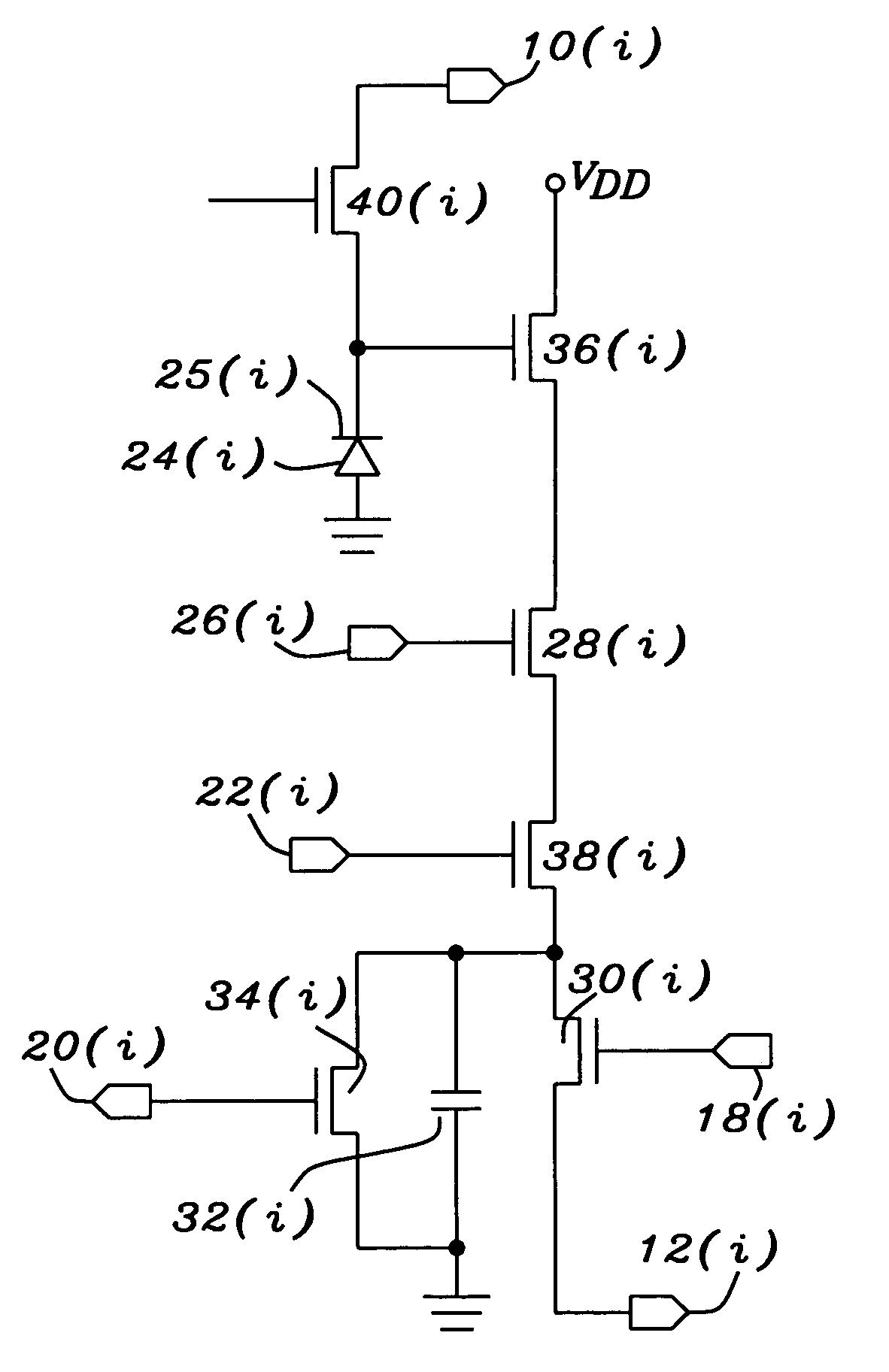
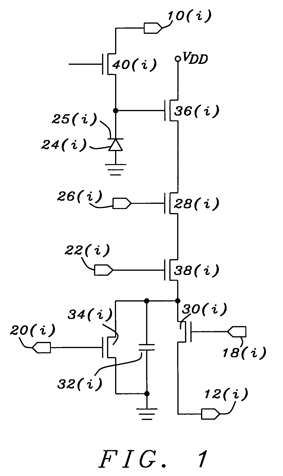
[0017]The circuits used in this invention are shown in FIGS. 1-2. FIG. 1 shows a schematic diagram of one of the sensor circuits of an imager. There can be a number of sensor circuits identical to the circuit shown in FIG. 1, each circuit indicated by the index (i). Typically there will be four such sensor circuits, although a larger or smaller number can be used, with i taking on values of 1, 2, 3, and 4. A photodiode 24(i) is used in each of the sensor circuits to integrate the charge generated by an input signal, such as a light signal, to produce an output signal. Typically, in the sensor circuits described by FIG. 1, each sensor circuit will have a different output signal, such as for different colors. The output of an output transistor 36(i), configured in source follower mode, is used to detect the output signal from the photodiode 24(i) and is fed to a sample and hold capacitor 32(i) by means of a row select transistor 28(i) and a sample transistor 38(i). The gate of the row...


PUM


Abstract

A circuit and method for reducing noise in video imagers which takes advantage of the fact that the same image information is present in the drain current in a reset transistor used to reset a photodiode in a pixel as is present in the readout current. The noise is reduced by passing the multiplexed output voltage from the source follower output transistor in an APS imager system through a high pass filter to reduce the low frequency noise from the source follower. The drain current in the reset transistor used to reset the APS is passed through a low pass filter. The low pass filter output and the high pass filter output are then combined. Since the drain current in the reset transistor contains the same image information as the voltage output of the source follower output transistor the image information can be obtained by combining the output of the low pass filter and the output of the high pass filter. Since the low frequency noise components of the source follower output transistor have been suppressed combined outputs of the low pass filter and high pass filter will provide the image information with greatly suppressed low frequency noise.

Description

[0001]This Patent Application claims priority to the following U.S. Provisional Patent Application, herein incorporated by reference:[0002]60 / 450,087, filed Feb. 26, 2003BACKGROUND OF THE INVENTION[0003](1) Field of the Invention[0004]The invention relates to a readout scheme for a CMOS Active Pixel Sensor, APS, that reduces 1 / f noise and low frequency fixed pattern noise.[0005](2) Description of the Related Art[0006]U.S. Pat. No. 4,831,451 to Hynecek describes a horizontal scannar having a plurality of stages. The scanner can be used for electronic zooming and panning operations.[0007]U.S. Pat. No. 4,764,814 to Endo et al. describes a solid state imaging device.[0008]U.S. Pat. No. 4,677,490 to Levine describes a CCD imager having a CCD output register having separate means for obtaining low frequency video response and high frequency video response. The low frequency response is obtained by sensing drain current in the output CCD line register. The high frequency response can be ob...

Claims


Application Information

Patent Timeline
Patent Type & Authority Patents(United States)
IPC IPC(8): H04N3/14H04N5/335H04N5/217H01L27/146H01L31/10H04N1/028H04N5/363H04N5/365H04N5/374H04N5/378
CPCH04N3/1568H04N5/335H04N5/3658H04N5/378H04N25/677H04N25/76H04N25/75G02F1/1303G02F1/1316
Inventor DOSLUOGLU, TANERLEVINE, PETER ALAN
Owner RPX CORP
Why Eureka
Try Eureka