Strained silicon with elastic edge relaxation

a technology of elastic edge relaxation and straining silicon, which is applied in the direction of basic electric elements, electrical apparatus, and semiconductor devices. it can solve the problems of reducing channel mobility, reducing channel mobility, and not being introduced to cmos manufacturing

Active Publication Date: 2008-03-04
ACORN TECH INC
View PDF13 Cites 36 Cited by
  • Summary
  • Abstract
  • Description
  • Claims
  • Application Information

AI Technical Summary

Problems solved by technology

However, despite much work on SiGe p-channel MOSFETs, such devices have not been introduced to CMOS manufacturing, at least in part due to the difficulty of forming a device quality gate oxide on a layer of SiGe.
To date this strategy has failed to eliminate propagation of threading dislocations into the subsequently grown strained silicon layer.
Threading dislocations represent extended defects and give rise to multiple undesirable consequences in MOSFETs including source / drain junction leakage, reduction of channel mobility, variability of threshold voltage and enhanced diffusion paths leading to potential drain-to-source shorting in short-channel MOSFETs.
Self heating has deleterious consequences for MOSFET performance such as increased off-state leakage current and mobility reduction leading to reduced drive current.
This has led to introduction of a CMP step to re-establish a planar surface, adding to cost of virtual substrate production.
The growth of a thick layer (for example, 2-3 microns) of graded SiGe, as used in forming strained silicon substrates according to the conventional process, has significant cost overhead.

Method used


Image

  • Strained silicon with elastic edge relaxation
  • Strained silicon with elastic edge relaxation
  • Strained silicon with elastic edge relaxation

Examples


Embodiment Construction

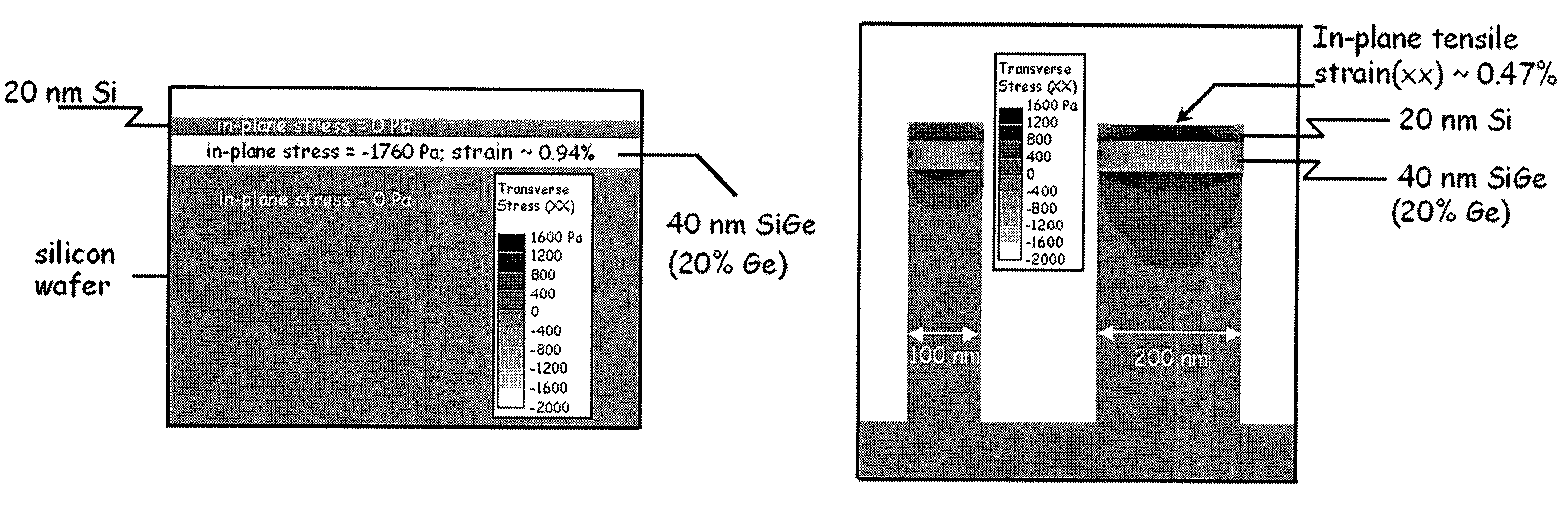
[0012]One aspect of the present invention provides a semiconductor device with a plurality of n-channel MOSFETs formed on a substrate. The substrate comprises silicon. Each of the n-MOSFET devices comprises a first layer comprising germanium formed over the substrate. The first layer has a thickness less than a first thickness at which misfit dislocations form in the first layer. The first layer has a first lower interface lattice spacing matched with a substrate interface lattice spacing characteristic of an interface region of the substrate. A second layer comprising silicon is formed over the first layer and the second layer has a second lower interface lattice spacing matched with a first layer upper interface lattice spacing characteristic of an upper interface of the first layer. A gate dielectric layer is provided on the second layer and separates the second layer from a gate electrode. A concentration of germanium in the first layer is greater than a concentration of germani...


PUM


Abstract

A thin blanket epitaxial layer of SiGe is grown on a silicon substrate to have a biaxial compressive stress in the growth plane. A thin epitaxial layer of silicon is deposited on the SiGe layer, with the SiGe layer having a thickness less than its critical thicknesses. Shallow trenches are subsequently fabricated through the epitaxial layers, so that the strain energy is redistributed such that the compressive strain in the SiGe layer is partially relaxed elastically and a degree of tensile strain is induced to the neighboring layers of silicon. Because this process for inducing tensile strain in a silicon over-layer is elastic in nature, the desired strain may be achieved without formation of misfit dislocations.

Description

FIELD OF THE INVENTION[0001]The present invention relates to stressed and strained layers in multilayer heterostructures containing silicon and germanium and more specifically relates to MOS devices formed in such heterostructures.DESCRIPTION OF THE RELATED ART[0002]Strained silicon is widely viewed as an important technology for obtaining desired advancements in integrated circuit performance. Biaxial, in-plane, tensile strained silicon exhibits enhanced in-plane electron and hole mobilities leading to improved n-channel and p-channel MOS field effect transistor (FET) performance relative to unstrained silicon. Mobility enhancement results from a combination of reduced effective carrier mass and reduced intervalley (phonon) scattering.[0003]Strained silicon is conventionally obtained by first growing a thick layer of silicon germanium alloy (SiGe) on a silicon substrate. The SiGe layer is grown to a sufficient thickness that the SiGe layer is relaxed to an unstrained condition at i...

Claims


Application Information

Patent Timeline
Patent Type & Authority Patents(United States)
IPC IPC(8): H01L21/00H01L21/336
CPCH01L29/1054H01L29/7846H01L29/66636H01L29/165H01L21/18H01L31/00
Inventor CLIFTON, PAUL A.
Owner ACORN TECH INC
Why Eureka
Try Eureka