Low-pressure removal of photoresist and etch residue

a technology of etch residues and photoresist, which is applied in the field ofplasma processing, can solve the problems of consuming the cap layer, reducing the efficiency of the process, so as to reduce the erosion of the remaining substrate layer

Active Publication Date: 2008-03-18
TOKYO ELECTRON LTD
View PDF6 Cites 38 Cited by
  • Summary
  • Abstract
  • Description
  • Claims
  • Application Information

AI Technical Summary

Benefits of technology

[0011]It is an object of the invention to provide a plasma processing method for removing photoresist remnants and etch residues from a substrate with reduced erosion of the surrounding substrate layers compared to one-step ashing.
[0013]During the first ashing step, where low or zero bias is applied to the substrate, a significant amount of photoresist remnants and etch residues on the substrate and internal surfaces / walls of the process chamber are etched and removed from the chamber, while erosion of the remaining substrate layers is minimized. During the second ashing step, an increased bias is applied and the ashing process is continued until the photoresist remnants and etch residues are removed.

Problems solved by technology

In semiconductor processing, where various types of films are etched, integration challenges and trade-offs still remain.
One of the integration challenges in plasma cleaning (also known as in-situ ashing), is to successfully remove photoresist remnants and etch residues, while avoiding erosion of surrounding layers.
As the bias is applied to the substrate holder, these fluorine radicals can erode the underlying dielectric film and consume the cap layer.

Method used


Image

  • Low-pressure removal of photoresist and etch residue
  • Low-pressure removal of photoresist and etch residue
  • Low-pressure removal of photoresist and etch residue

Examples


Embodiment Construction

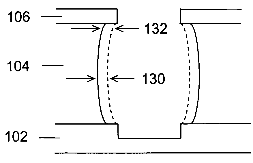
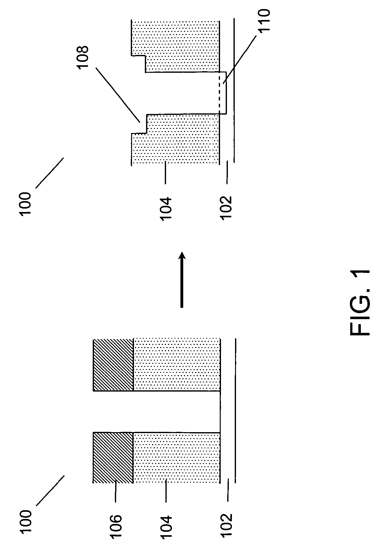
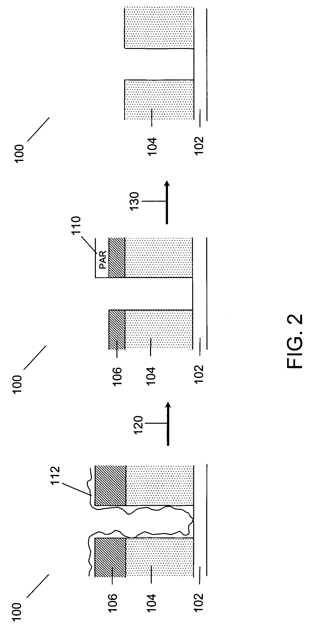
[0022]The inventors of related U.S. patent application Ser. No. 10 / 259,381, entitled METHOD FOR REMOVING PHOTORESIST AND ETCH RESIDUE, which are the inventors of the present application, realized that a two-step plasma ashing process can be utilized to remove photoresist remnants and etch residues from a substrate. During the first ashing step, where zero or low bias is applied to a substrate holder upon which a substrate resides, a significant amount of photoresist remnants and etch residues, from preceding etch processes that can, for example, utilize CxFy etch gases, are etched and removed from the processing chamber with minimal erosion of the remaining substrate layers. During the second ashing step, an increased bias is applied to the substrate holder and the ashing process is continued until the photoresist and / or hard mask remnants, and post-ash residues are removed.

[0023]The current inventors have realized that the above-mentioned two-step plasma ashing process can be impro...


PUM


Abstract

A method is provided for plasma ashing to remove photoresist remnants and etch residues formed during preceding plasma etching of dielectric layers. The ashing method uses a two-step plasma process involving a hydrogen-containing gas, where low or zero bias is applied to the substrate in the first cleaning step to remove significant amount of photoresist remnants and etch residues from the substrate, in addition to etching and removing detrimental fluorocarbon residues from the chamber surfaces. An increased bias is applied to the substrate in the second cleaning step to remove the remains of the photoresist and etch residues from the substrate. A chamber pressure less than 20 mTorr is utilized in the second cleaning step. The two-step process reduces the memory effect commonly observed in conventional one-step ashing processes. A method of endpoint detection can be used to monitor the ashing process.

Description

CROSS-REFERENCE TO RELATED APPLICATIONS[0001]The present application is related to co-pending U.S. patent application Ser. No. 10 / 259,381, filed on Sep. 30, 2002, the entire contents of which are herein incorporated by reference. The present application is related to copending U.S. patent application entitled “LOW-PRESSURE REMOVAL OF PHOTORESIST AND ETCH RESIDUE”, filed on Dec. 30, 2004, the entire contents of which are herein incorporated by reference.FIELD OF THE INVENTION[0002]The present invention relates to plasma processing, particularly to cleaning and removal of photoresist and etch residues following an etching process in semiconductor microfabrication.BACKGROUND OF THE INVENTION[0003]Plasma processing systems are used in the manufacture and processing of semiconductors, integrated circuits, displays and other devices or materials, to both remove material from or to deposit material on a substrate such as a semiconductor substrate. Plasma processing of semiconductor substra...

Claims


Application Information

Patent Timeline
Patent Type & Authority Patents(United States)
IPC IPC(8): H01L21/302
CPCH01J37/32082H01L21/02063H01L21/31138G03F7/427H01J2237/3342H01L22/26H01L21/302
Inventor BALASUBRAMANIAM, VAIDYANATHANHATAMURA, YASUNORIHAGIHARA, MASAAKINISHIMURA, EIICHIINAZAWA, LEGAL REPRESENTATIVE, RIEINAZAWA, KOICHIRO
Owner TOKYO ELECTRON LTD
Why Eureka
Try Eureka