Method of manufacturing semiconductor device including air space formed around gate electrode

a gate electrode and air space technology, applied in the field of semiconductor device manufacturing, can solve the problems of reducing the electrical characteristics of the device in a high frequency range, and achieve the effects of reducing parasitic capacitance, excellent electrical characteristic, and high frequency rang

Inactive Publication Date: 2008-04-15
MITSUBISHI ELECTRIC CORP
View PDF8 Cites 0 Cited by
  • Summary
  • Abstract
  • Description
  • Claims
  • Application Information

AI Technical Summary

Benefits of technology

[0010]It is an object of the present invention to provide a method of manufacturing a semiconductor device which is capable of reducing a parasitic capacitance to provide an excellent electrical characteristic in a high frequency range.
[0012]The method reduces the parasitic capacitance to provide the semiconductor device exhibiting the excellent electrical characteristic in the high frequency range.
[0014]The method reduces the parasitic capacitance to provide the semiconductor device exhibiting the excellent electrical characteristic in the high frequency range.
[0016]The method reduces the parasitic capacitance to provide the semiconductor device exhibiting the excellent electrical characteristic in the high frequency range.

Problems solved by technology

As a result, the conventional HEMT presents a problem in that the parasitic capacitances result in the reduction in electrical characteristics of the device in a high frequency range.

Method used


Image

  • Method of manufacturing semiconductor device including air space formed around gate electrode
  • Method of manufacturing semiconductor device including air space formed around gate electrode
  • Method of manufacturing semiconductor device including air space formed around gate electrode

Examples


first preferred embodiment

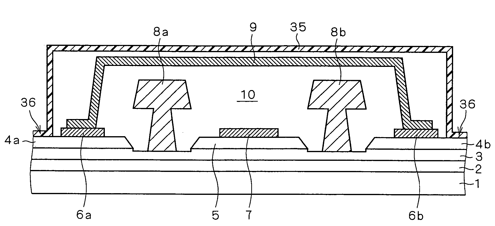
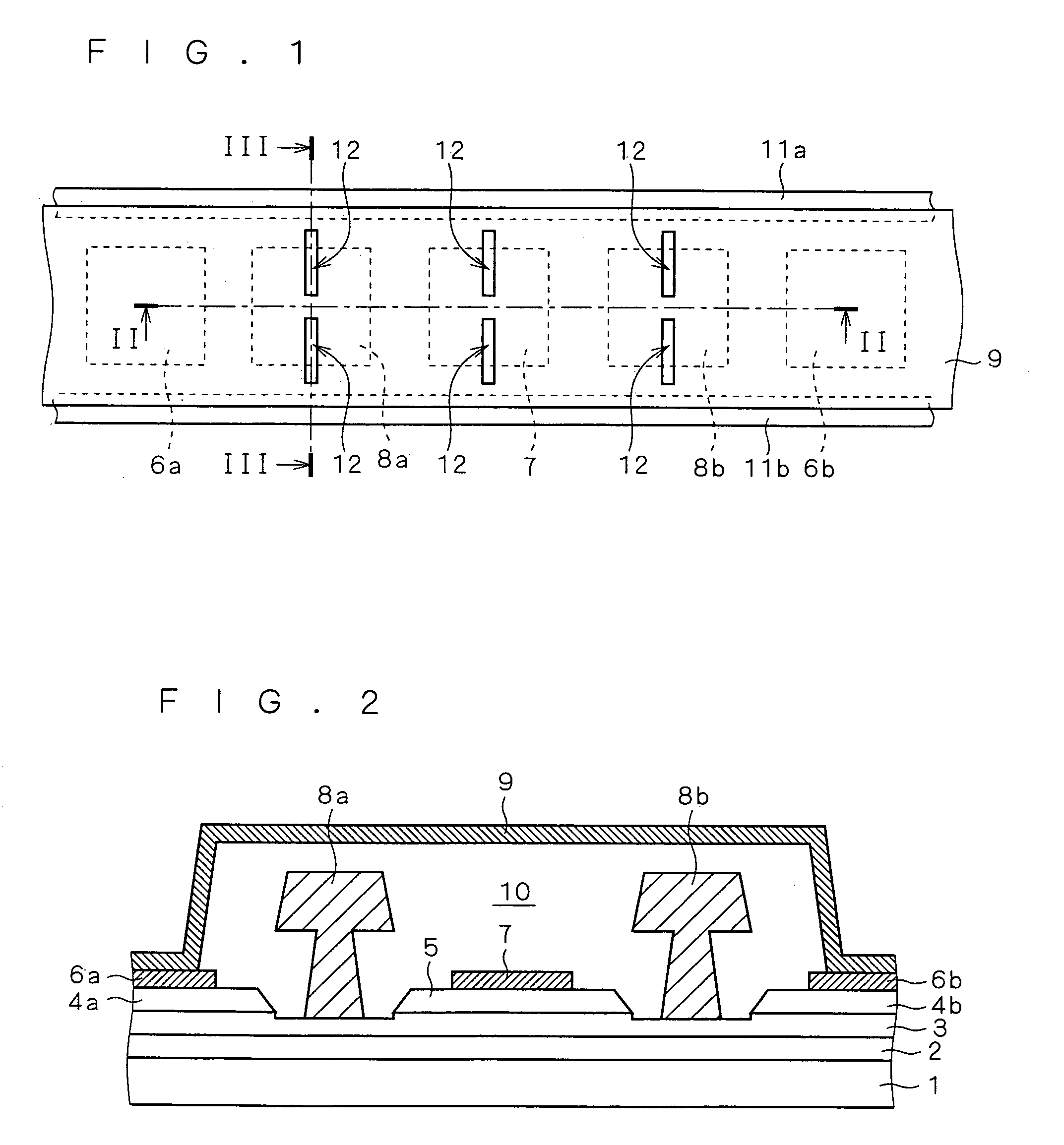
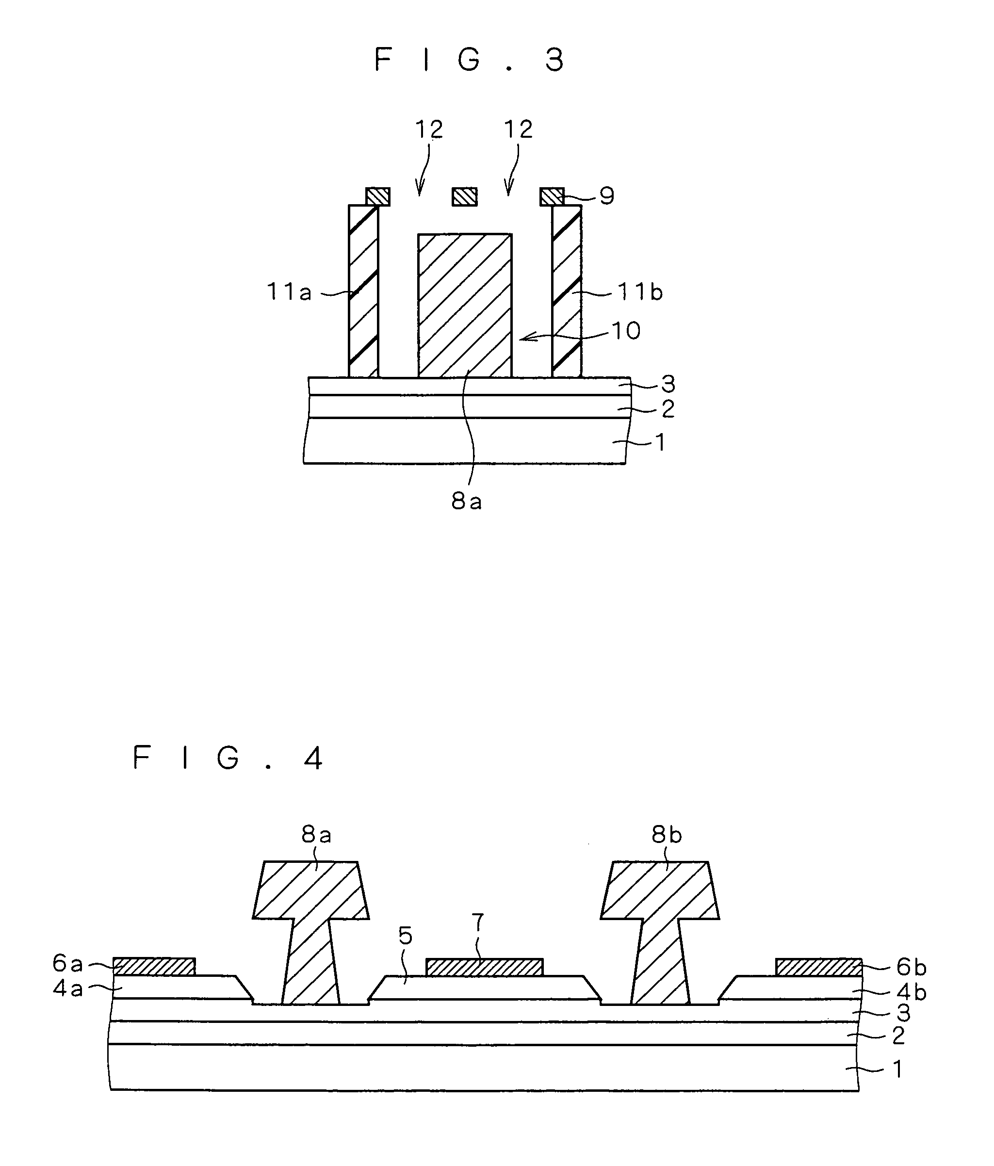
[0040]FIG. 1 is a top plan view showing a structure of a semiconductor device according to a first preferred embodiment of the present invention. FIGS. 2 and 3 are sectional views showing sectional structures taken along the lines II-II and III-III, respectively, of FIG. 1.

[0041]With reference to FIG. 2, a HEMT according to the first preferred embodiment includes a compound semiconductor substrate 1 such as a GaAs substrate, an electron transit layer 2, an electron supply layer 3, heavily doped layers 4a, 4b and 5, source electrodes 6a and 6b, a drain electrode 7, and gate electrodes 8a and 8b having an overhanging shape. The electron transit layer 2 is formed on the entire surface of the compound semiconductor substrate 1. The electron supply layer 3 is formed on the entire surface of the electron transit layer 2. The heavily doped layers 4a, 4b and 5 are formed partially on the electron supply layer 3 in spaced-apart relation to each other. The compound semiconductor substrate 1, ...

second preferred embodiment

[0056]FIGS. 13 and 14 are sectional views corresponding to FIGS. 2 and 3, respectively, and showing structures of the semiconductor device according to a second preferred embodiment of the present invention. An insulation film 20 made of Ta2O5, BST, STO or the like is formed on the metal interconnect line 9, and the slits 12 are closed by the insulation film 20.

[0057]After the structures shown in FIGS. 2 and 3 are provided, a CVD process or an evaporation process is used to deposit or evaporate the insulation film 20 on the entire surface of the metal interconnect line 9. The size of each of the slits 12 is, for example, as follows: 1 μm in width and 20 μm in length. The thickness of the insulation film 20 is, for example, 3 μm. Because of the very small width of the slits 12, the insulation film 20 being deposited or evaporated does not enter the interior of the slits 12 but is formed to span over the slits 12 in the step of forming the insulation film 20. As a result, the insulati...

third preferred embodiment

[0059]FIGS. 15 and 16 are schematic views showing the method of manufacturing the semiconductor device in a step-by-step manner according to a third preferred embodiment of the present invention.

[0060]With reference to FIG. 15, a liquid resin 23 having a high viscosity such as a polyimide or the like is stored in a liquid tank 24. A wafer 25 formed with the structures shown in FIGS. 2 and 3 is supported by a support rod 26, with the metal interconnect line 9 positioned to face downward (that is, with the structures of FIGS. 2 and 3 turned upside down). The wafer 25 in this position is dipped into the liquid resin 23. Thus, the liquid resin 23 is applied to the surface of the metal interconnect line 9. The wafer 25 may be spin-coated with the liquid resin 23, rather than being dipped into the liquid resin 23.

[0061]With reference to FIG. 16, after the wafer 25 is taken out of the liquid resin 23, the wafer 25 is opposed to a hot plate 27, with the metal interconnect line 9 positioned ...


PUM


Abstract

After a HEMT is formed, side walls are formed on a semiconductor substrate. Next, a sacrificial layer is formed to cover the HEMT. Next, contact holes are formed in the sacrificial layer to expose upper surfaces of source electrodes. Next, a metal interconnect line is formed by patterning a metal film formed on the entire top surface. Next, slits are formed in the metal interconnect line to partially expose an upper surface of the sacrificial layer. After the sacrificial layer is dissolved, the dissolved sacrificial layer is discharged through the slits to the outside. An air space is formed as a result of the removal of the sacrificial layer.

Description

BACKGROUND OF THE INVENTION[0001]1. Field of the Invention[0002]The present invention relates to a method of manufacturing a semiconductor device and, more particularly, to a method of manufacturing a transistor operating at high frequencies.[0003]2. Description of the Background Art[0004]In recent years, electronic circuits operating at high frequencies have been in dramatically increasing demand because of the worldwide expansion of the market for mobile communication equipment typified by portable telephones and the like and the rapid proliferation of satellite communication services. Additionally, with the increase in the amount of transmitted information, there has been a need for communication at higher frequencies. To meet such requirements, MMICs (Monolithic Microwave Integrated Circuits) operating at high frequencies in the microwave region and for the formation on compound semiconductor substrates have been developed actively.[0005]Of the MMICs, particularly important devi...

Claims


Application Information

Patent Timeline
Patent Type & Authority Patents(United States)
IPC IPC(8): H01L21/4763H01L21/44
CPCH01L21/764H01L27/0605
Inventor OGAWA, TETSUYAKITANO, TOSHIAKIMINAMI, HIROYUKI
Owner MITSUBISHI ELECTRIC CORP
Why Eureka
Try Eureka