Gem tester using electrical photoconductivity

a technology of electrical photoconductivity and gem tester, which is applied in the direction of resistance/reactance/impedence, measurement devices, instruments, etc., can solve the problems of time, time, and time consumption, and achieve the effect of reducing the effect of the object being tested, reducing the cost of operation, and improving safety and comfort for users

Inactive Publication Date: 2008-04-22
TRI ELECTRONICS
View PDF12 Cites 21 Cited by
  • Summary
  • Abstract
  • Description
  • Claims
  • Application Information

AI Technical Summary

Benefits of technology

[0010]Thermal conductivity is estimated by the speed at which preheated copper probe cools down when it touches the object under test. The cooling process is affected by many causes, some of which cannot be controlled or easily accounted for. To achieve reliable estimate of thermal conductivity in presence of unknown factors we used differential method by employing two temperature sensors. One, measurement sensor, which is closer to the tested object, is used for sensing the effects caused by the tested object while the other, reference sensor, which is separated from the tested object by the heating element, accounts for all other influences. The reference signal is subtracted from the measurement signal resulting in more robust and reproducible estimates.
[0012]The electrical portion was modified and upgraded to meet increasing challenge and to provide better reliability, productivity, safety, and convenience.
[0014]Our observations demonstrated that moissanites possess significant photoconductivity, which means that electrical current caused by applying voltage across the stone increases sharply when the stone is exposed to sufficiently bright light of sufficiently short wavelength. While this effect may be difficult to notice in better conducting stones, in the high-resistance stones, which have small electrical conductivity, the photocurrent becomes the dominant part of electrical current. We incorporated in our device a high intensity white light emitting diode (LED), which is placed in the tip above the probe. This LED is turned on when no significant ‘dark’ electrical conductivity is found. This expands significantly the range of diamond look-alikes that can be detected.
[0019]In summary, our invention uses the lowest test voltage for the least time, resulting in minimal effect on the objects being tested, better safety and comfort for the user, and smaller power consumption.
[0020]Measurement circuit from the source of the test voltage goes through the operator's body, then through the metal of the ring or the test plate, then through the gem to the probe, which is connected to the amplifier input. AC interference enters the circuit from the operator's body, in the described measurement circuit the interference signal is divided in the same proportion as the test voltage in the resistive divider, which includes the gem under test. This prevents the interference signal from becoming a dominant component of the small test signal when dealing with high resistance gems.
[0021]To further reduce the error caused by AC interference, measured signal is rid of industrial pick up, which normally is the main part of the interference. This is achieved by averaging a sufficient number of evenly distributed samples over 0.1 sec. This time interval contains a whole number of cycles of 50, 60, 100, and 120 Hz, which are the frequencies of industrial AC and of rectified power voltage in different countries. Averaging over whole number of cycles of a periodic signal results in removal of the periodic components below alias frequency.

Problems solved by technology

The cooling process is affected by many causes, some of which cannot be controlled or easily accounted for.
Another problem associated with thermal measurements using hot probe is the time, which is required to preheat the probe.
This delay every time the device is turned on is annoying and counterproductive.

Method used


Image

  • Gem tester using electrical photoconductivity
  • Gem tester using electrical photoconductivity
  • Gem tester using electrical photoconductivity

Examples


Embodiment Construction

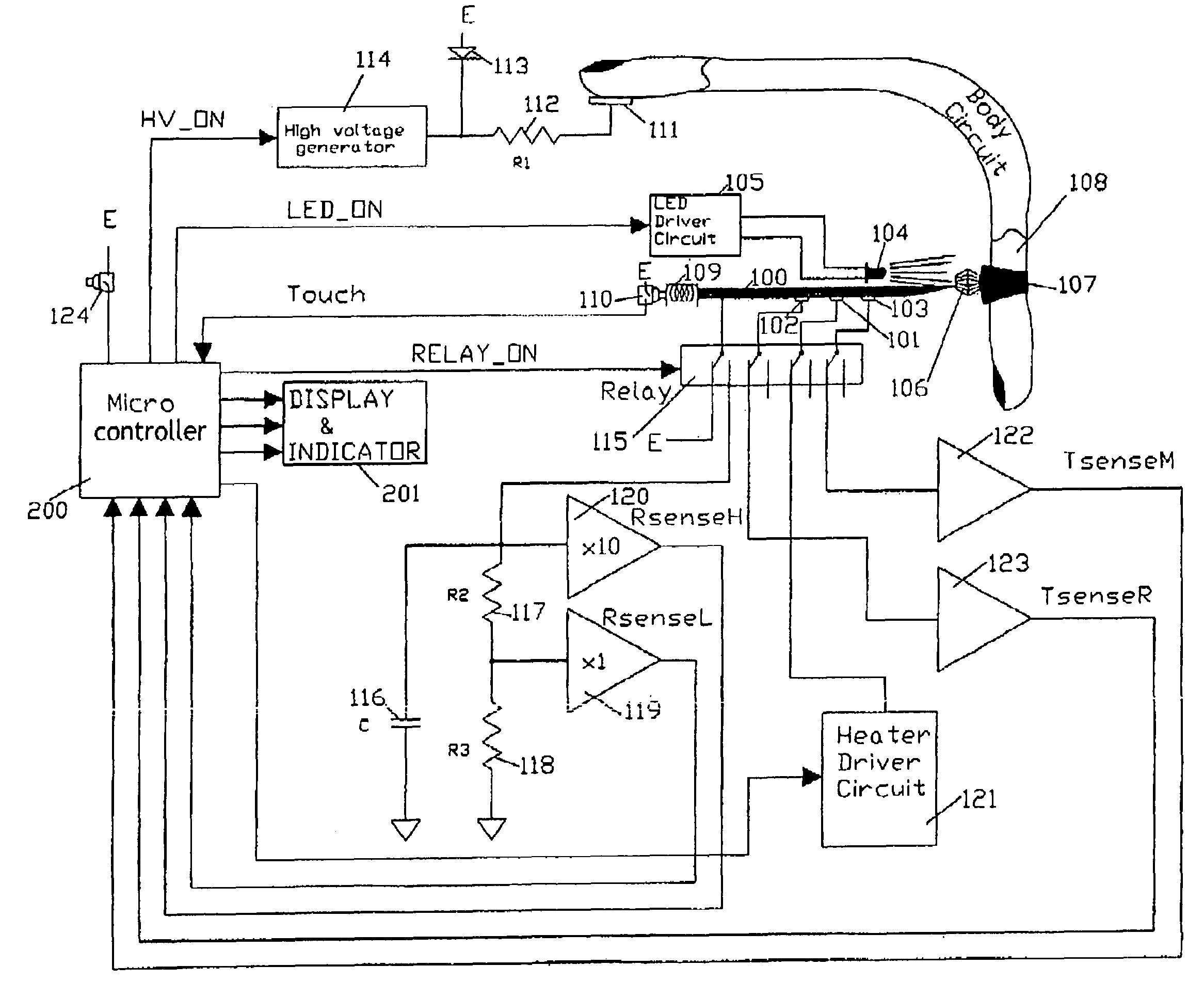
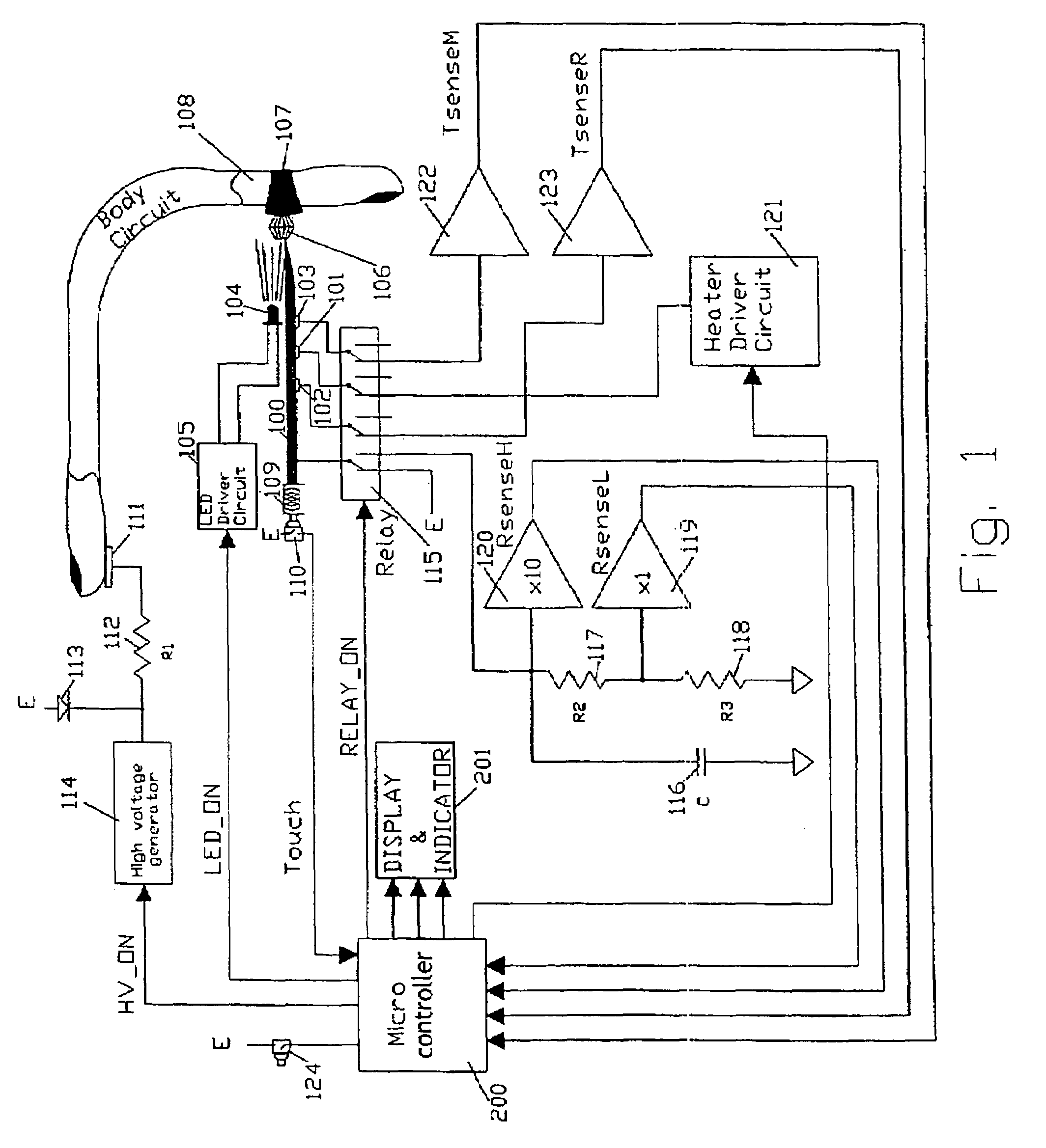
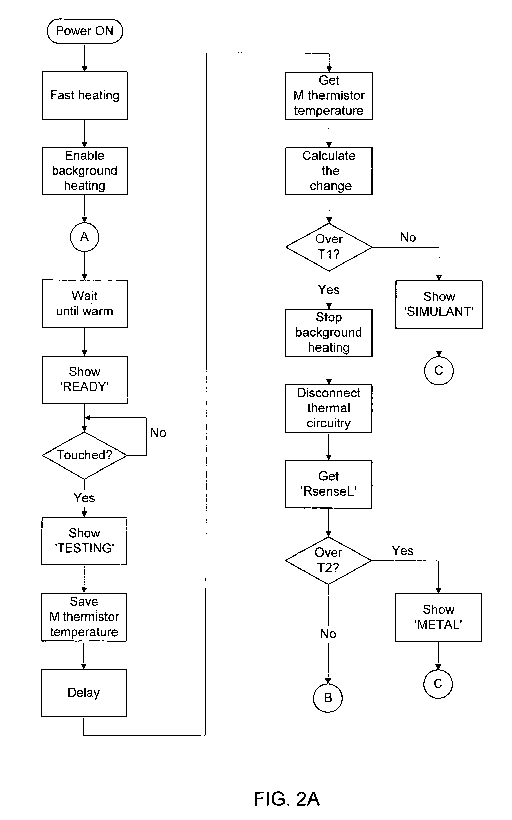
[0026]As other successful diamond testers on the market, present invention employs both thermal and electrical conductivity testing for the purpose of determining reliably whether the stone being testied is a natural diamond.

[0027]It should be noted that this device does not actually establish if the object, which is being tested, is a diamond, a moissanite, a synthetic diamond, or, say, cubic zirconium. Such positive identifications would require more sophisticated equipment and longer testing. The device just evaluates thermal and electrical conductivities. By the results of these measurements tested objects are determined as following. Those with electrical conductivity above certain threshold are announced as metal. Those with thermal conductivity below certain threshold are diagnosed as simulants. These may include cubic zirconium, some synthetic gems, plastics, or glass. Those with high thermal conductivity are diagnosed as diamonds when electrical conductivity is below certai...


PUM


Abstract

Diamond look-alikes like cubic zirconium, moissanite and other synthetic stones, are distinguishable from nature diamonds based on their thermal and / or electrical conductivities. Germ testers that are on the market are capable of evaluating these two parameters as is the present invention. Electrical resistance of moissanites reaches hundreds of thousands megohms. Existing gem esters use test voltage of 1000 volts, to be able to detect electrical conductivity in most moissanites. Still, reliable detection of high resistance moissanites is difficult. Proposed invention uses significant photo conductivity of moissanites, which was observed by the inventors, to facilitate measurement of electrical conductivity in the toughest gems, to reduce test voltage applied to gems to 300 volts, and to limit electrical test current through a gem to no more than a few micro-amps. Other refinements include: (1) multistep evaluation of electrical conductivity, which avoids applying excessive or unnecessary test voltage and current to a gem, (2) circuit design, which efficiently attenuates AC noise, (3) signal processing, which eliminates industrial pick-up, (4) usage of reference temperature sensor, which improves sensibility and repeatability of thermal measurements.

Description

RELATED APPLICATION[0001]This application claims the benefit of U.S. Provisional Application Ser. No. 60 / 619,576 filed on Oct. 18, 2004 entitled “Using Electrical Photoconductivity to Distinguish High-resistance Moissanites from Natural Diamonds,” the entire teachings of which are herein incorporated by reference.BACKGROUND OF THE INVENTION[0002]The old task of distinguishing diamonds look-alikes from natural diamonds continues to be important. However this task becomes ever more difficult as quality of synthetic gems, which are partially indistinguishable from natural diamonds with the naked eye, improves and their characteristics, which could be used for the purpose of distinguishing them from natural diamonds, approach those of natural diamonds.[0003]Two techniques, which are usually used in portable diamond testers, are based on diamonds' exceptionally high thermal conductivity and their high electrical insulation ability. Those diamond look-alikes that have similar electrical i...

Claims


Application Information

Patent Timeline
Patent Type & Authority Patents(United States)
IPC IPC(8): G01R27/08
CPCG01N27/041
Inventor LOGINOV, BORIS ZOLOTAR
Owner TRI ELECTRONICS
Why Eureka
Try Eureka